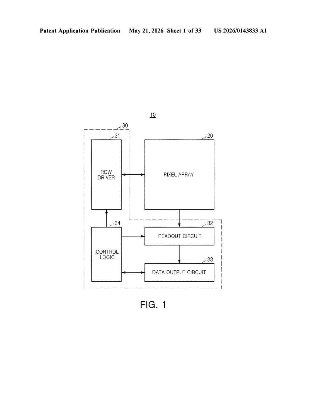
Samsung Patents a Dual-Node Image Sensor with Built-In Gain Control
Samsung is patenting a smarter way to read out light from a camera sensor — one that lets each pixel group independently tune how it handles bright and dark signals at the hardware level.
What Samsung's dual floating diffusion sensor actually does
Imagine taking a photo in a scene that has both a very bright window and a dimly lit corner. Most camera sensors struggle here: they're calibrated for one exposure level, so either the bright parts blow out or the dark parts go muddy.
Samsung's patent describes an image sensor where each group of pixels contains two types of photodiodes — a primary one and a secondary one — each connected to its own separate charge-storage node. A set of transistors, including a dedicated gain control transistor, lets the circuit adjust how much signal is amplified before it gets sent out. Think of it like having a tiny volume knob inside every pixel cluster.
By switching between nodes and tuning the gain on the fly, the sensor can handle a much wider range of light levels without needing software tricks after the fact. That could mean cleaner high-dynamic-range images straight from the hardware.
How the pixel circuit routes charge between two diffusion nodes
The patent describes a pixel array made up of pixel groups, each containing multiple photodiodes arranged in a grid. Within each group, photodiodes are split into two roles: primary photodiodes (likely the main light-capturing elements) and secondary photodiodes (likely smaller or differently tuned ones for capturing overflow charge or a different exposure level).
The key innovation is the dual floating diffusion node architecture. A floating diffusion node (FD) is the tiny capacitor-like region that collects the electrical charge produced when light hits a photodiode — it's the handoff point before the signal is amplified. Here, there's a first FD node tied to the primary photodiode via a transfer transistor, and a second FD node tied to the secondary photodiode. A first switch transistor sits between the two FD nodes, letting the circuit combine or isolate their charges.
What makes the circuit distinctive is the series combination of a reset transistor and a gain control transistor sitting between a power supply and the first FD node. By controlling that gain transistor, the circuit can change the effective capacitance at the node — which directly controls amplification sensitivity (higher capacitance = lower gain = handles brighter light; lower capacitance = higher gain = captures dim light better).
- A capacitor + second switch transistor pair on the second FD node adds further tunable storage.
- An amplification transistor reads the voltage at the first FD node and drives the output.
- A select transistor gates the output onto the column readout line, as is standard in CMOS image sensor design.
What this means for Samsung's next camera sensors
For Samsung, which competes fiercely in the mobile camera sensor market against Sony's IMX series, incremental improvements to per-pixel dynamic range and noise performance are genuinely meaningful. A sensor that can tune its gain at the pixel-circuit level — rather than relying purely on multi-exposure stacking in the ISP — could reduce motion blur artifacts that haunt HDR photography.
This is also relevant for machine vision and automotive camera applications, where consistent performance across wildly varying lighting conditions matters more than megapixel count. If Samsung can integrate this kind of flexible readout into future ISOCELL sensors, it's a quiet but real improvement to the imaging pipeline that every phone using one of their sensors would benefit from.
This is solid, incremental image sensor engineering — not a headline-grabbing concept but exactly the kind of pixel-circuit refinement that separates good sensors from great ones. Samsung is clearly investing in hardware-level HDR capability, and this patent is a credible piece of that puzzle. It won't make news at a product launch, but it's the kind of building block that compounds over time.
Get one Big Tech patent every Sunday
Plain English, intelligent commentary, no hype. Free.
Editorial commentary on a publicly published patent application. Not legal advice.