Sony Patents a Lattice-Matched Substrate Design for Cleaner micro-LED Displays
Most micro-LED displays are plagued by tiny crystal defects introduced when the semiconductor is moved off its original growth substrate. Sony's patent describes keeping that substrate in place — and making sure it matches the crystal structure perfectly.
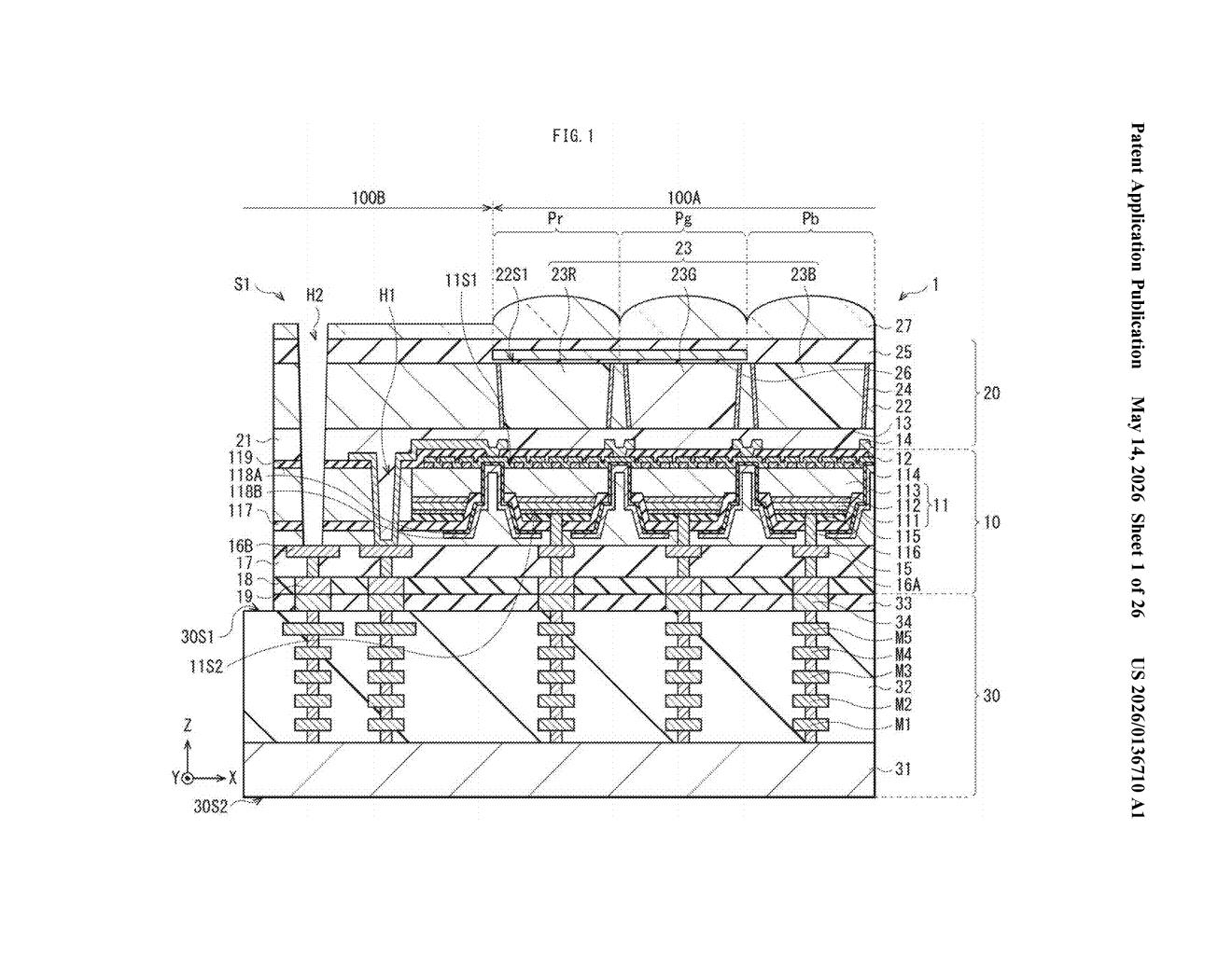
What Sony's growth-substrate micro-LED structure actually does
Imagine building a tiny Lego tower on a base plate where every stud lines up perfectly. Now imagine trying to move that tower to a different base plate where the studs don't quite match — some bricks crack, some connections weaken. That's basically the problem Sony is trying to solve in miniature LED displays.
In micro-LED screens, each pixel is a tiny semiconductor chip that glows when electricity hits it. Normally, manufacturers grow those chips on one surface and then transfer them to a driver board. That transfer can introduce crystal mismatches — microscopic stress points that cause defects and reduce brightness or lifespan.
Sony's approach keeps the original growth substrate — the surface the LEDs were literally grown on — attached to the light-outputting side of the display. Because the substrate was grown to match the LED crystal structure exactly, there's no mismatch stress. You end up with a cleaner, potentially more reliable display stack.
How Sony's lattice-matched interface eliminates crystal defects
The patent describes a three-layer sandwich structure for a light-emitting display device:
- Drive substrate — the bottom layer, containing the transistors that power each pixel.
- Light-emitting elements — an array of compound semiconductor LEDs (think gallium nitride or similar materials) sandwiched in the middle, each with a bottom face touching the driver and a top face that outputs light.
- Growth substrate — the top layer, left in contact with the light-outputting surface of every LED in the array.
The critical detail is that the growth substrate forms an interface free of lattice mismatch with the compound semiconductor. Lattice mismatch refers to a difference in the atomic spacing between two crystalline materials — when two crystals with different spacings are bonded, the resulting strain can generate defects called dislocations that degrade device performance.
By retaining the original substrate rather than transferring the LEDs to a foreign carrier, Sony's design avoids introducing those stress points entirely. The growth substrate was engineered alongside the LED material from the start, so the atomic grids line up.
This is essentially a substrate-retained or native-substrate architecture, as opposed to the more common transfer printing or pick-and-place micro-LED manufacturing process where LEDs are lifted off their growth substrate and deposited elsewhere.
What this means for Sony's micro-LED display ambitions
The micro-LED display industry has been chasing commercialization for years, and crystal defects introduced during the transfer process remain one of the hardest manufacturing problems to crack. If Sony can skip the transfer step while maintaining electrical performance, you'd theoretically get better yield, longer pixel lifespans, and reduced manufacturing complexity — all of which translate to lower costs over time.
Sony's semiconductor division supplies display technology for everything from professional monitors to AR/VR headsets. A cleaner micro-LED substrate process could be significant for next-generation high-brightness, high-efficiency display panels — especially in compact form factors where defect density matters most.
This is a solid, focused materials-engineering patent that addresses a real bottleneck in micro-LED manufacturing. It's not a flashy AI story, but lattice mismatch is a genuine problem that has slowed micro-LED commercialization for years — Sony's native-substrate approach is a credible engineering response worth tracking.
Get one Big Tech patent every Sunday
Plain English, intelligent commentary, no hype. Free.
Editorial commentary on a publicly published patent application. Not legal advice.