Microsoft Patents a Chip Circuit That Runs Complex Math in Fewer Steps
Deep inside every AI chip, the same arithmetic operations repeat billions of times per second. Microsoft's latest patent tries to shave time off one of those repeating loops by fusing two separate hardware units into one.
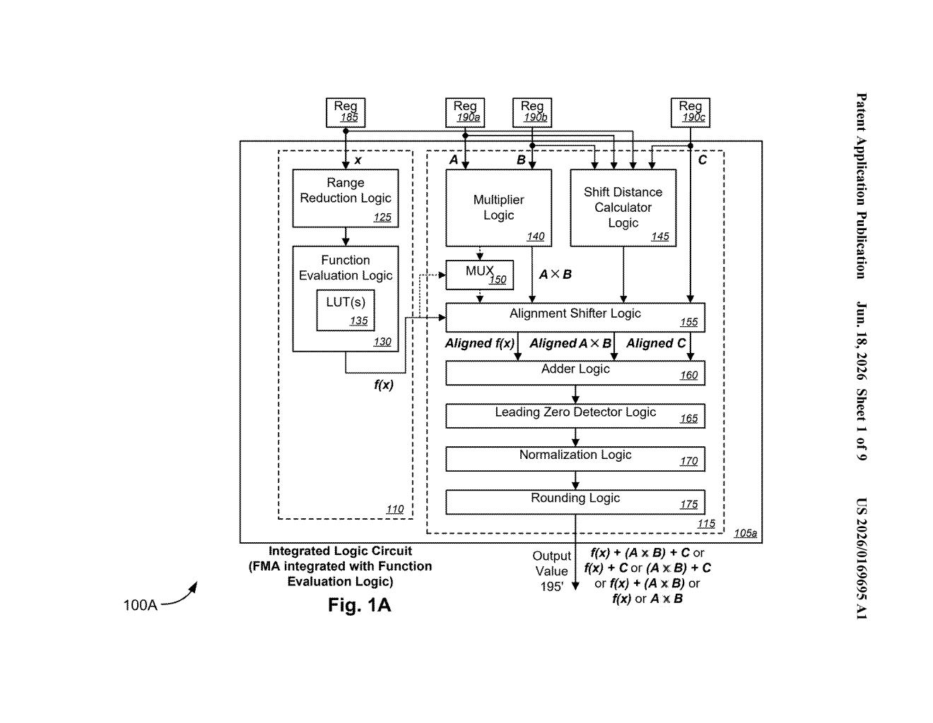
What Microsoft's fused math circuit actually does
Imagine a factory assembly line where two workers each finish their task and then hand their results to a third worker who adds them together. Now imagine collapsing that into one workstation where the addition happens the moment either worker is done. That's roughly the idea here.
Right now, chips that do AI math run complex operations — like calculating a square root or a logarithm — in one circuit, then pass the result to a separate addition circuit. Each handoff takes time. Microsoft's patent describes a circuit design where the function-calculation step and the addition step are physically fused, so the adder can receive results directly, without waiting for an intermediate stop.
The patent covers what engineers call a fused multiply-add (FMA) circuit — a workhorse of AI and graphics math — extended to also handle functions like exponentials or logarithms in the same integrated unit. One input goes in, one rounded output comes out, with fewer internal delays along the way.
How the FMA and function logic share one adder
The patent describes an integrated logic circuit that combines two things that are usually separate on a chip: a fused multiply-add (FMA) unit (a standard building block that multiplies two numbers and adds a third in one step, which is faster than doing it in two) and a function evaluation unit (hardware that computes things like exponentials, logarithms, or trigonometric values).
Normally, if a chip needs to compute, say, exp(x) + y, it would run the exponential in one circuit, store the result, then pass it to an adder. Each storage-and-pass step costs clock cycles. This patent's circuit skips that intermediate storage: the function evaluation logic feeds its output directly and concurrently into the adder within the same FMA unit.
The sequence the patent describes is:
- A first value (the function's variable, e.g., x) enters the function evaluation logic
- The function logic computes a second value (e.g., exp(x))
- The adder simultaneously receives that second value and a third value (e.g., y) — no waiting
- The adder produces a fourth value (the sum), which then goes through normalization and rounding to produce the final output
Normalization and rounding are the cleanup steps that convert raw binary arithmetic results into properly formatted floating-point numbers — the format chips use for decimals. Doing all of this in one integrated unit reduces the number of times intermediate results have to be written and re-read inside the chip.
What this means for AI chip efficiency
AI models — whether generating text, processing images, or running recommendations — rely heavily on functions like softmax and layer normalization, which are built from exponentials and logarithms. Those functions currently require extra hardware cycles every time they run. A chip circuit that fuses function evaluation directly into the FMA pipeline could reduce latency and power draw for those operations at scale.
Microsoft operates some of the world's largest AI infrastructure through Azure, and has been investing in custom silicon. A more efficient FMA-plus-function circuit would be most valuable in AI accelerators and neural network processors, where the same math operations repeat across millions of neurons. Even small per-operation savings compound into meaningful performance gains when multiplied across billions of daily inference calls.
This is a solid piece of low-level chip engineering that probably won't make headlines outside of hardware circles — but that's exactly where AI performance gets won or lost. The idea of fusing function evaluation into an FMA isn't entirely new as a concept, but Microsoft patenting a specific implementation suggests this is heading toward real silicon, likely for Azure AI accelerators. Worth tracking if you follow Microsoft's custom chip ambitions.
Get one Big Tech patent every Sunday
Plain English, intelligent commentary, no hype. Free.
Editorial commentary on a publicly published patent application. Not legal advice.