Samsung Patents a New Metal Alloy for the Wires Inside Its Chips
The tiny wires inside a computer chip are one of the biggest bottlenecks in modern electronics — and Samsung thinks a new metal alloy could help fix that.
What Samsung's new chip wiring alloy actually does
Imagine a city where all the roads are getting narrower as the buildings get taller. That's roughly what's happening inside modern chips: as transistors shrink, the metal wires connecting them have to shrink too, and the materials that worked fine at larger sizes start causing serious problems.
Samsung is patenting a new metal alloy — a mix of metals including molybdenum or tungsten combined with niobium or vanadium — to use as those wires. The idea is that this combination holds up better at tiny scales than the copper wiring used in chips today, which can become unreliable and inefficient as it gets thinner.
This is the kind of materials-science work that happens deep in the chip-making process, invisible to you as a user, but it's the sort of incremental advance that makes future phones, laptops, and AI processors possible.
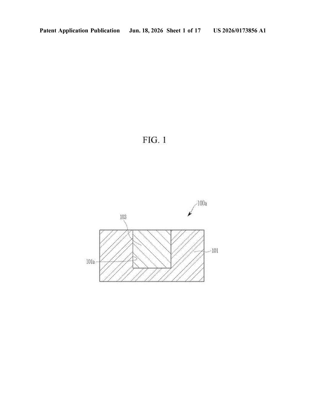
How the molybdenum-niobium alloy fills chip trenches
Inside a chip, electrical signals travel through interconnects — microscopic metal wires embedded in an insulating (dielectric) layer. As chip features shrink below a few nanometers, copper, the traditional wiring metal, develops serious problems: its electrical resistance shoots up, and it can physically degrade over time.
Samsung's patent describes a conductive wiring layer made from a specific alloy family. The alloy pairs a base metal — either molybdenum (Mo) or tungsten (W), both refractory metals known for stability at small scales — with a secondary metal: either niobium (Nb) or vanadium (V). The ratio is controlled so the secondary metal stays below 50% of the mix (x < 0.5 in the chemical formula).
The wiring is deposited inside trench structures — tiny grooves etched into the insulating dielectric layer. Filling those trenches uniformly with this alloy, rather than copper, is what the patent is specifically claiming. The tunable alloy composition lets engineers dial in the right balance of conductivity, adhesion, and thermal stability for a given chip design.
Key elements covered:
- Base metals: Molybdenum, tungsten, or both
- Dopant metals: Niobium, vanadium, or both
- Form factor: Fills etched trenches in a dielectric insulating layer
- Composition limit: Secondary metal fraction kept below 50%
What this means for smaller, faster Samsung chips
The chip industry has been hunting for copper replacements for years, and molybdenum-based alloys have emerged as a serious candidate. If Samsung can produce interconnects with this alloy reliably at manufacturing scale, it could enable denser, lower-power chips — which eventually shows up as longer battery life or faster performance in the devices you buy.
That said, this is a materials patent covering a broad alloy family, not a finished manufacturing process. Samsung is staking out intellectual property in a competitive space where Intel, TSMC, and others are also experimenting with next-generation wiring metals. Whether this specific alloy makes it into mass production is a separate question entirely.
This is a narrow but real piece of semiconductor infrastructure work — exactly the kind of patent that doesn't make headlines but quietly shapes what chips look like five years from now. The molybdenum-based interconnect space is genuinely competitive, and Samsung filing here is a meaningful signal that it's investing in post-copper wiring at the materials level. Not exciting reading, but worth tracking.
Get one Big Tech patent every Sunday
Plain English, intelligent commentary, no hype. Free.
Editorial commentary on a publicly published patent application. Not legal advice.