
Nvidia Patents a Way to Stop Multi-Chip GPUs from Talking Over Each Other
When a GPU is spread across two chips, every time one chip needs to tell the other something, that conversation takes time. Nvidia's new patent is about making each chip mind its own business as much as possible.
What Nvidia's split-GPU memory trick actually does
Ever noticed how a busy office slows down when everyone has to cc the whole team on every email? A GPU split across two chips faces exactly that problem: every small update one chip sends to the other adds a tiny delay, and in graphics processing those delays pile up fast.
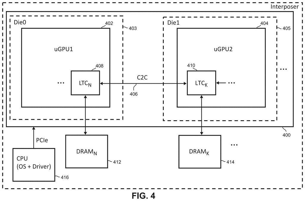
Nvidia's patent describes a system where each chip in a multi-chip GPU writes its own rendering setup data (things like how vertices and surfaces should look) to its own local memory, without needing to broadcast that information to the other chip. Each side handles its portion of the screen independently, only reaching across when it truly has to.
The result is less cross-chip chatter, lower wait times for each chip, and a more efficient use of the connection between the two dies. It's a form of careful traffic management baked into the hardware itself.
… the first rendering hardware writing first rendering parameters to first point of coherence memory locally connected to the first die without requiring writes over the chip-to-chip communication interface to the second die …
Translation: Each chip saves its data locally instead of bothering the others.
How each chip writes to its own local memory slice
The patent covers a multi-chip GPU where two separate processor dies each handle a portion of the final image, a technique called tile-based rendering. Each die is responsible for its own rectangular slice of the screen.
The core idea is localization: instead of writing shared rendering parameters (settings like vertex attributes, which define the shape and position of 3D geometry, or constants that control shading) to a shared pool that both chips access, each die writes those values only to the memory physically connected to itself. The patent calls these "point of coherence" memories, meaning each chip's local memory is the authoritative copy for its own work.
The system also localizes:
- Page pool and root table version buffers (internal bookkeeping structures that track how virtual memory is organized)
- Local memory used by individual rendering threads
All of this sits on top of a coarse-grained interleaved virtual memory layout, meaning the overall memory space is divided into large alternating chunks assigned to each chip, rather than fine-grained byte-by-byte interleaving. Each chip's local writes stay in its own chunk, so the chip-to-chip link (the physical wire connecting the two dies) is only used when genuinely necessary, not for every small write operation.
… localizing writes of certain graphics pipeline attributes, localizing certain page pool and root table version buffers, and/or localizing of local memory in order to improve the latency of write operations and/or to reduce the inter-chip traffic in a multi-chip graphics processing unit …
Translation: Keeping tasks on their home chips speeds things up and cuts down on chatter between them.
What this means for high-end GPU performance and design
Multi-chip GPU designs are one of the main ways the industry is pushing past the physical limits of how large a single chip can be. But splitting a GPU across two dies introduces a real bottleneck: the connection between them is slower and more energy-hungry than on-chip memory access. Every unnecessary byte sent across that link costs performance.
This patent directly attacks that bottleneck. By keeping routine rendering data local to whichever chip needs it, Nvidia can reduce the latency of common operations and cut down the bandwidth used by the chip-to-chip link. For you as a user, that could translate into higher frame rates or more headroom for complex scenes in applications that push GPU limits, like high-resolution 3D rendering or real-time simulation.
Nvidia's 35th filing we've tracked since July in the GPU rendering race builds on one about routing graphics data between chips and one about growing small textures into full images.
Cross-chip communication in a multi-chip graphics processor works like a highway toll: every small write that crosses the boundary between chips costs time, and graphics workloads generate enormous volumes of small writes. That tax compounds quickly as GPUs grow more complex.
Nvidia's answer is to identify specific categories of data that never actually need to cross that boundary and simply keep them local. Vertex attributes, constants, and per-thread memory all qualify, and rerouting them removes overhead without touching the underlying architecture.
The approach matches the problem well precisely because it is narrow rather than ambitious. A targeted fix for a structural bottleneck tends to age better than a sweeping redesign, and this one addresses a cost that only grows as chips get larger.
There are more where this came from
We read every patent application Big Tech publishes and send you the ones worth knowing. Plain English, free, every week.
The drawings
22 drawing sheets from US 2026/0288335 A1 · click any drawing to enlarge


Want this weekly breakdown for a company we don't cover? Patentlyze Pro →
Be the first to weigh in