Samsung Patents a Way to Route Chip Data Through Ordinary CPU Registers
Most chips need special instructions to feed data to an AI accelerator. Samsung's new patent skips the custom plumbing entirely by hijacking a regular CPU register.
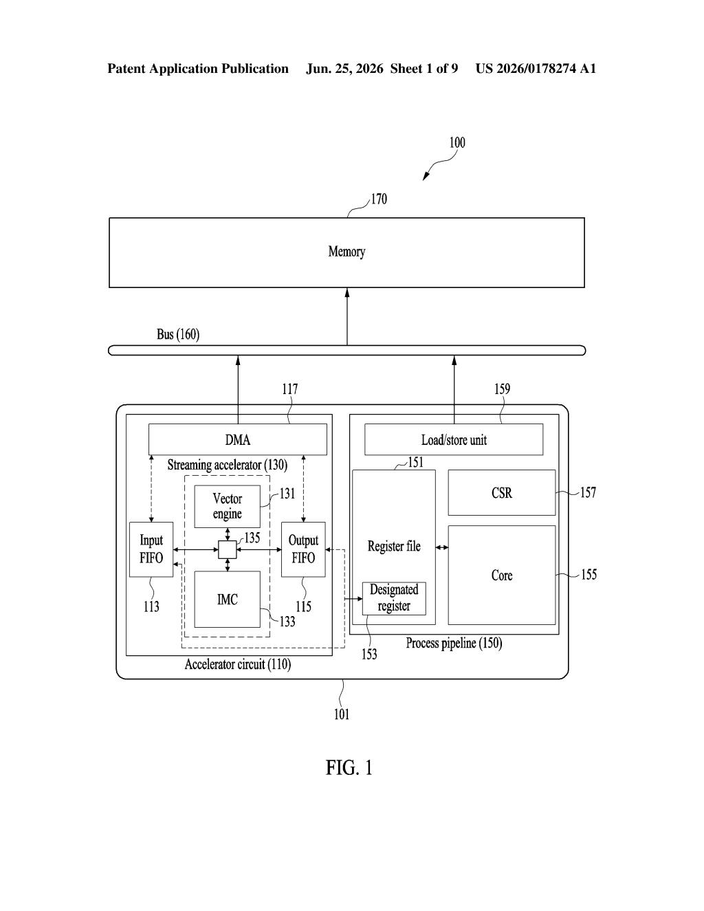
How Samsung's processor talks to its accelerator chip
Imagine your laptop's main brain and its dedicated AI chip as two offices that need to pass documents to each other. Normally you'd need a special courier with a custom badge just for that hallway. Samsung's patent proposes using the regular mail slot that everyone already has, so no new courier is needed.
The trick is that the main processor designates one of its ordinary working slots (called a register) as a special pass-through. When the chip reads from or writes to that slot, the data automatically flows into or out of a queue on the accelerator instead of going to regular memory.
For you, this means chips built this way could be simpler to program and potentially cheaper to make, because software written for a standard processor can already reach the accelerator without learning new commands.
How the CSR-to-FIFO pipeline actually moves data
The patent describes a processor design where a control and status register (CSR) (a small configuration switch baked into the processor core) is used to promote one of the chip's standard general-purpose registers into a streaming pointer. Think of a streaming pointer as a labeled pipe: once assigned, any normal memory-read or memory-write instruction that names that register gets silently redirected.
Instead of hitting main memory, those redirected instructions go straight into the input or output FIFO buffer of a streaming accelerator. A FIFO (first-in, first-out) buffer is simply a waiting line: data enters one end in order and exits the other end in the same order. This is standard for feeding continuous streams of numbers, like neural network weights, to dedicated compute units.
The key architectural move is that the core's instruction set architecture (ISA) (the public rulebook for what instructions a chip understands) does not need to be changed. Existing load and store instructions do the work; the CSR setting tells the hardware to treat one register differently.
- CSR sets which register becomes the streaming pointer
- Load instruction targeting that register pulls from the accelerator's output FIFO
- Store instruction targeting it pushes to the accelerator's input FIFO
What this means for Samsung's custom chip ambitions
Samsung is building its own processor cores (Exynos series) and neural processing units for phones, servers, and automotive chips. Making the CPU-to-accelerator interface work through standard instructions rather than custom extensions means existing compilers and software tools can target the accelerator without modification, which cuts the engineering cost of adopting the hardware.
It also reduces the number of dedicated instructions that need silicon area and verification time. If Samsung ships this in a future Exynos or data-center chip, you'd see the benefit indirectly: faster on-device AI with less software overhead, and potentially shorter development cycles for the apps and firmware that run on top of it.
This is a tidy piece of microarchitecture housekeeping, not a headline-grabbing invention. The real value is in the toolchain story: by keeping the ISA clean, Samsung makes its accelerators easier to adopt across different software stacks. It's the kind of patent that matters inside a chip design team.
Get one Big Tech patent every Sunday
Plain English, intelligent commentary, no hype. Free.
Editorial commentary on a publicly published patent application. Not legal advice.