
Qualcomm Patents a Method to Stack Different Processor Chips Across Multiple Levels
Qualcomm has filed a patent for a chip design that stacks processing cores on top of each other in three dimensions, letting different types of processors share the same package without being crammed onto a single flat layer of silicon.
What Qualcomm's 3D chip stacking actually means for devices
Why does your phone sometimes feel sluggish running demanding apps even when the chip inside looks impressive on paper? One big reason is that all the processing muscle, the memory, and the supporting hardware have to share a flat, limited slab of silicon.
Qualcomm's new patent proposes a different approach: instead of laying everything side by side, stack multiple chip layers on top of each other, the way you'd stack floors in a building. Each layer, called a die, handles certain jobs, and they all talk to each other through a shared connection in the middle. One layer might run the main processing cores; another might handle memory or a specialized type of processor entirely.
The key twist is that the connecting interface is designed to welcome different types of processor cores, not just one fixed family. So the chip can mix and match the right kind of processor for a given task, all within the same stacked package.
a first die configured with a first set of functionalities; an interface that supports different types of processor architectures; and at least one additional die having one or more processor cores of one of the different types of processor architectures …
Translation: A base chip connects to an interface that links up various kinds of processor architectures stacked right on top.
How the stacked dies share cores and memory across layers
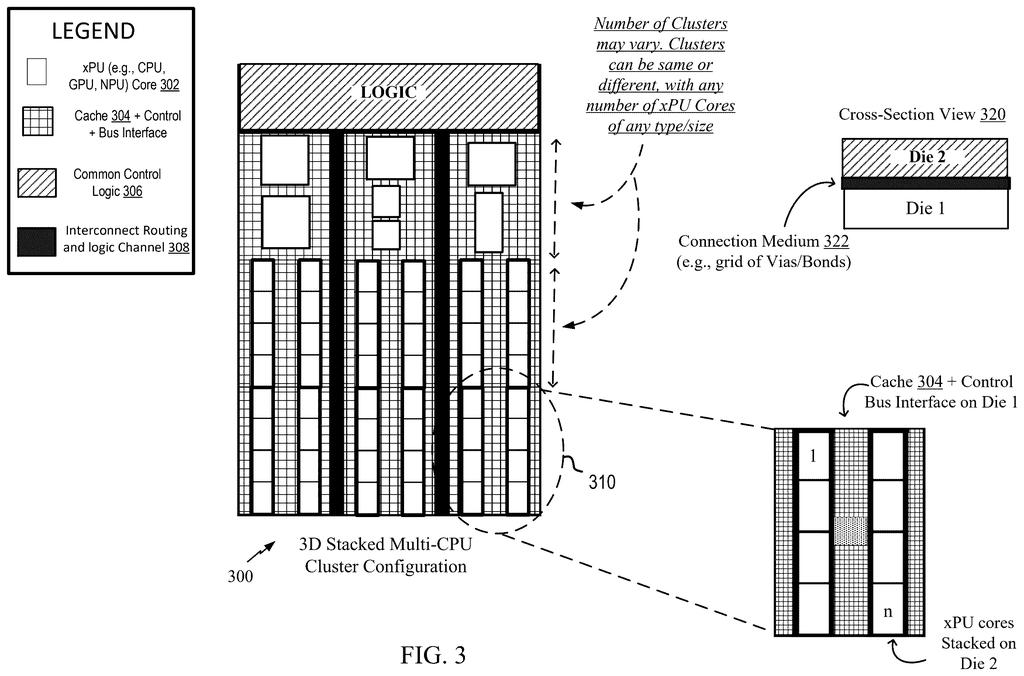
The patent describes a three-dimensional stacked processing unit, a chip assembly where multiple silicon layers (called dies) are bonded together vertically rather than spread across a single flat chip.
Here is how the pieces fit together:
- A first die holds a core set of shared functions, things like memory controllers or communication logic that other layers need to reach.
- An interface layer sits between the dies and acts as a translator and traffic director. Crucially, it is designed to support different processor architectures, meaning chips built around different design philosophies can all plug into it and use those shared functions.
- One or more additional dies each carry processor cores of a specific type. Those cores reach down through the interface to use whatever the first die provides, whether that is cache memory, data pathways, or control logic.
The interface doing the heavy lifting here (supporting multiple processor architectures, not just one) is what separates this from a simple chip-on-chip stack. It means a future device could, in theory, house a general-purpose CPU core on one layer and a specialized AI or signal-processing core on another, all sharing the same foundation without redesigning the entire chip.
… at least one processing unit, comprising one or more processing cores and cache memory, distributed across at least two of the first die and the one or more additional dies …
Translation: Processing cores and memory are spread out across multiple stacked layers of chips.
What this means for future phones, laptops, and AI chips
The chip industry is running into a physical wall: you can only shrink transistors so far before the laws of physics push back hard. Stacking chips in three dimensions is one of the main paths forward, and Qualcomm's approach here adds flexibility by making the stacking interface compatible with different processor types. That matters because modern devices need several different kinds of processors (ones for general tasks, ones for AI, ones for radios) and traditionally each has lived on its own separate chip.
If this architecture reaches production, it could mean more capable chips in the same physical space, which is directly relevant to smartphones, AR glasses, and any wearable where size is the enemy. It could also reduce the energy wasted when data has to travel long distances between separate chips on a circuit board.
Qualcomm's 50th filing we've tracked in the AI chip wars since July builds on earlier work like its memory-side processing patent and its lean on-device AI method.
The problem this patent attacks is real and expensive. As chips get more complex and single-layer designs hit physical limits, the industry has been forced to find creative ways to pack more power into smaller packages. Three-dimensional stacking is already being pursued by Intel, AMD, and TSMC, so Qualcomm is working in well-established territory here.
What gives this filing some texture is the multi-architecture interface. Most stacked chip designs assume all the layers will speak the same processor language. Designing the interface to handle different architectures is a harder problem, and solving it would make the approach far more flexible for companies that need to mix CPU, AI, and radio cores in one tight package.
That said, the patent is fairly abstract at this stage. It lays out the concept without deep detail on how the interface actually negotiates between competing architectures in practice. Qualcomm's bet on heterogeneous processor design shows up across multiple filings, and this one fits that pattern, but whether this particular approach becomes a shipping product or stays a paper concept is an open question.
There are more where this came from
We read every patent application Big Tech publishes and send you the ones worth knowing. Plain English, free, every week.
The drawings
7 drawing sheets from US 2026/0277810 A1 · click any drawing to enlarge


Want this weekly breakdown for a company we don't cover? Patentlyze Pro →