
Qualcomm Patents a Dual-Method System for Letting Memory Chips Handle Their Own Processing
Most computer chips shuffle data back and forth to memory constantly, wasting energy and time. Qualcomm's new patent describes a way to keep more of that work inside the memory chip itself, by giving it its own address system.
What Qualcomm's dual-address memory system actually does
You're running a demanding AI task on your phone or laptop, and the processor is drowning in data it has to pull from memory, crunch, then push back. That constant back-and-forth is slow and eats battery.
Qualcomm's patent tackles this with a concept called process-in-memory, or PIM, where the memory chip does some of the math itself instead of waiting for the main processor. The catch is that today's chips use a single address system to find data in memory, and that system is optimized for normal reads and writes, not for the kind of localized work PIM needs to do.
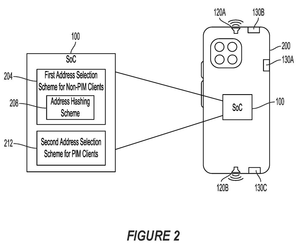
The patent describes giving PIM operations their own separate addressing scheme. Normal requests use the standard system; PIM requests use a different one, tuned to how the memory chip likes to organize its own internal work. Think of it like having one postal system for national mail and a different one for packages that never leave the building.
… process-in-memory (PIM) circuitry coupled to the one or more memories, the memory device configured to: receive, by the memory device, a first request in accordance with a first address selection scheme that includes an address hashing scheme …
Translation: The chip uses special circuitry to handle two different types of incoming requests using separate address rules.
How the two address schemes split normal and PIM traffic
The patent describes a processing system (the main chip) that talks to a memory device capable of running its own internal computations. Normally, memory addresses are scrambled using a technique called address hashing, which spreads data evenly across memory banks to avoid bottlenecks when multiple requests arrive at once.
That spreading is great for normal traffic, but it's a problem for PIM. When the memory chip tries to do math on a block of data, it needs that data to be sitting in one predictable, local spot inside itself. Hashing scatters it everywhere, which defeats the point.
- First address scheme: standard hashed addressing, used for regular read/write requests from the processor.
- Second address scheme: a different scheme, selected specifically when the request involves PIM operations, keeping data localized so the memory chip can process it efficiently.
The system detects whether a given memory request is a normal one or a PIM one, then routes the address through the appropriate scheme. That detection and switching logic lives in both the processing system that sends requests and the memory device that receives them, so both sides stay in sync on which addressing rules apply.
In accordance with the second request being associated with process-in-memory (PIM) operations by the memory device, the second physical address is in accordance with a second address selection scheme different than the first address selection scheme.
Translation: Requests for internal memory processing follow a completely different addressing path than standard memory requests.
What this means for AI chips and memory-heavy workloads
For AI workloads, especially on mobile devices, getting memory operations right is one of the biggest levers on performance and battery life. Qualcomm keeps filing around in-memory and near-memory computing as AI tasks migrate from data centers to the chips inside phones and wearables. A cleaner handoff between the processor and PIM-capable memory could mean faster inference without draining your battery as fast.
That said, PIM hardware is still a fairly specialized piece of equipment. This patent is really about the software and signaling layer that sits between a standard processor and a PIM-capable memory chip. The value only materializes if both sides of that conversation exist in the same device, which means the real question is when PIM memory becomes a standard component rather than a research curiosity.
Qualcomm's 49th filing we've tracked in AI chip wars since July adds to a pattern that includes work on running leaner AI block by block and fixing errors in compressed models.
On the path to a shipping product, this patent describes a coordination layer, not new hardware. It assumes the hard part, a memory chip that can run its own computations, already exists and focuses on how a processor should address and speak to that chip without confusion.
That makes the shortest route to a product something like: build the PIM memory first, then use this addressing scheme as the handshake that lets standard processors treat it correctly. The filing is closer to a protocol than a breakthrough, which is not a knock against it. Protocols are what turn capable hardware into something a product team can actually ship.
The real signal for anyone watching AI chips is that Qualcomm is doing the plumbing work early. Getting the communication rules right before the memory exists at scale is exactly how useful technology moves from a research demo to something in a device.
There are more where this came from
We read every patent application Big Tech publishes and send you the ones worth knowing. Plain English, free, every week.
The drawings
8 drawing sheets from US 2026/0277821 A1 · click any drawing to enlarge


Want this weekly breakdown for a company we don't cover? Patentlyze Pro →