Samsung Patents a Dual-Waveguide Design for Controlling Light in Chips
Light-based chips are becoming a serious alternative to copper wiring inside data centers, and Samsung is filing the underlying plumbing that makes them work — starting with a new way to control light pulses at the chip level.
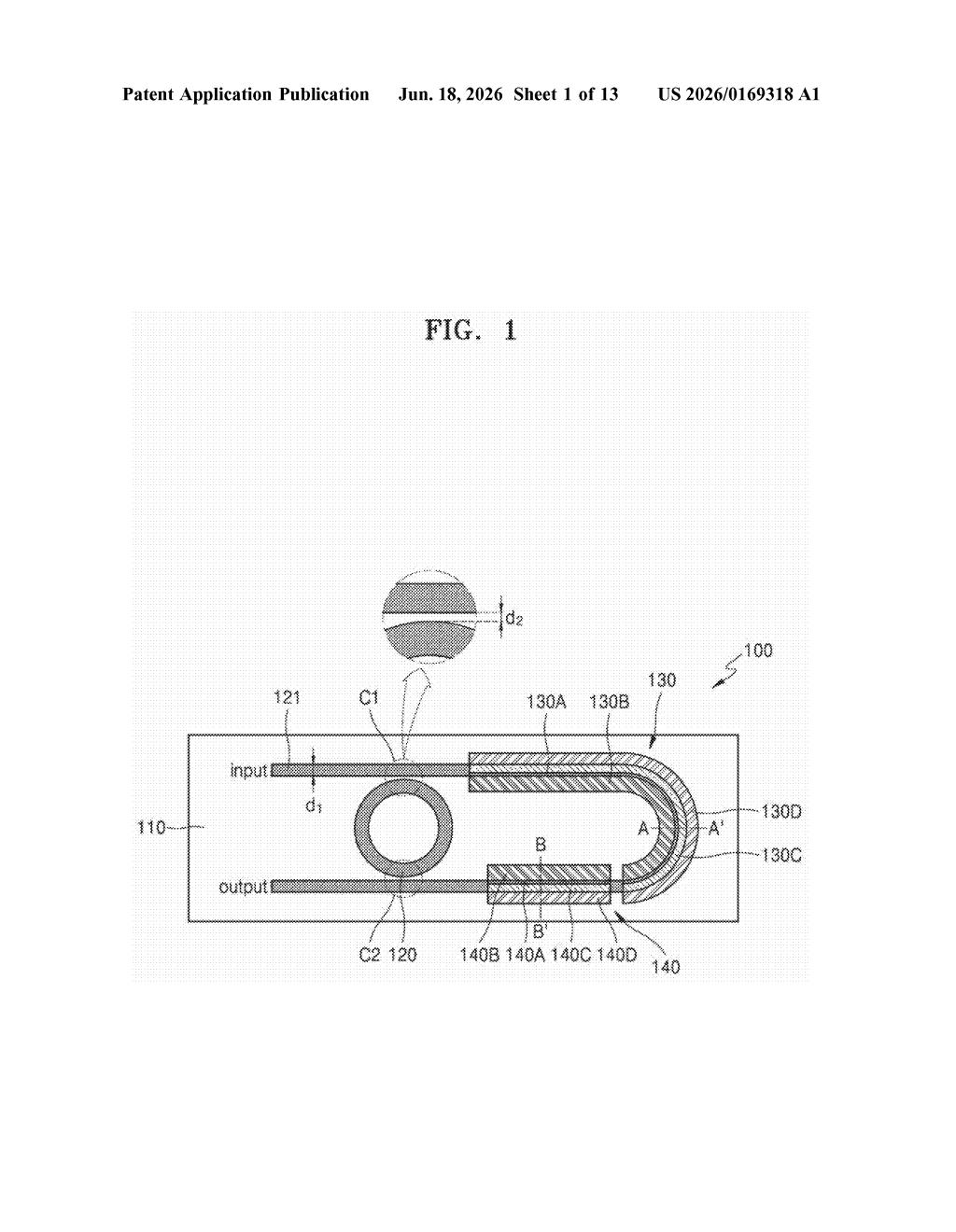
What Samsung's ring-and-U light modulator actually does
Imagine a fiber-optic cable, but shrunk down to fit inside a computer chip. Instead of copper wires carrying electricity, these chips use pulses of light to move data — much faster and with less heat. To make that work, you need a device called a modulator, which acts like a very fast light switch, turning signals on and off billions of times per second.
Samsung's patent describes a new modulator design that uses two interlocked waveguides — tiny channels that guide light the way a pipe guides water. One is shaped like a ring; the other is shaped like the letter U and wraps around two sides of the ring. The points where they get close enough to touch are where the light "couples," or transfers between the two channels.
By splitting the switching work across two separate sections of the U-shaped guide, Samsung's design could control light pulses more precisely than a single-point approach. It's the kind of foundational hardware patent that doesn't make headlines on its own, but could quietly show up inside future optical networking chips.
How the ring and U-shaped waveguides couple together
The patent covers an optical modulator — a device that encodes data onto a beam of light by rapidly changing the light's properties (like its phase or intensity). Modulators are essential building blocks in silicon photonics, the field that puts fiber-optic-style communication onto ordinary semiconductor chips.
The specific architecture here combines two waveguides:
- A first optical waveguide shaped like a closed ring — similar to the ring resonators already common in photonic chips, which work by trapping and amplifying specific light frequencies.
- A second optical waveguide shaped like a U, positioned so that each arm of the U runs alongside one side of the ring, creating two distinct coupling regions where the ring and U waveguide interact.
Each arm of the U contains its own modulation unit — essentially an electrode or voltage-controlled section that can shift the light passing through it. Because the two modulation units act on light at different points around the ring, the design gives engineers two separate "handles" to tune the modulator's behavior.
The two coupling regions (where ring meets U) let light transfer between the two waveguides in a controlled way. Tuning both modulation units together — or independently — provides finer control over the output signal compared with a simple single-bus ring modulator.
What this means for optical chips and data-center speeds
Silicon photonics is increasingly important for data centers, where moving enormous amounts of data between processors and memory with copper wires is becoming a bottleneck. Optical modulators are one of the hardest components to miniaturize and tune, so improvements to their geometry can have real downstream effects on how fast and efficient these interconnects become.
For you as an end user, this kind of patent sits several layers below anything you'd directly touch — but it feeds into the infrastructure that determines how quickly AI models train, how fast cloud services respond, and how much energy a data center burns. Samsung is a major semiconductor manufacturer, and filing photonics IP signals it wants a seat at that table.
This is a narrow, structural patent covering one specific waveguide geometry — not a system patent and not a product announcement. It's genuine technical work in an area (silicon photonics) that actually matters for the next decade of computing, but on its own it's a single brick, not a building. Worth tracking if you follow optical interconnect IP; easy to skip if you don't.
Get one Big Tech patent every Sunday
Plain English, intelligent commentary, no hype. Free.
Editorial commentary on a publicly published patent application. Not legal advice.