
Samsung Files Patent for Zone-by-Zone AI Defect Detection on Silicon Wafers
Samsung is patenting a system that trains a different AI model for each physical region of a silicon wafer, betting that defects cluster by location and that one-size-fits-all quality checks leave money on the table.
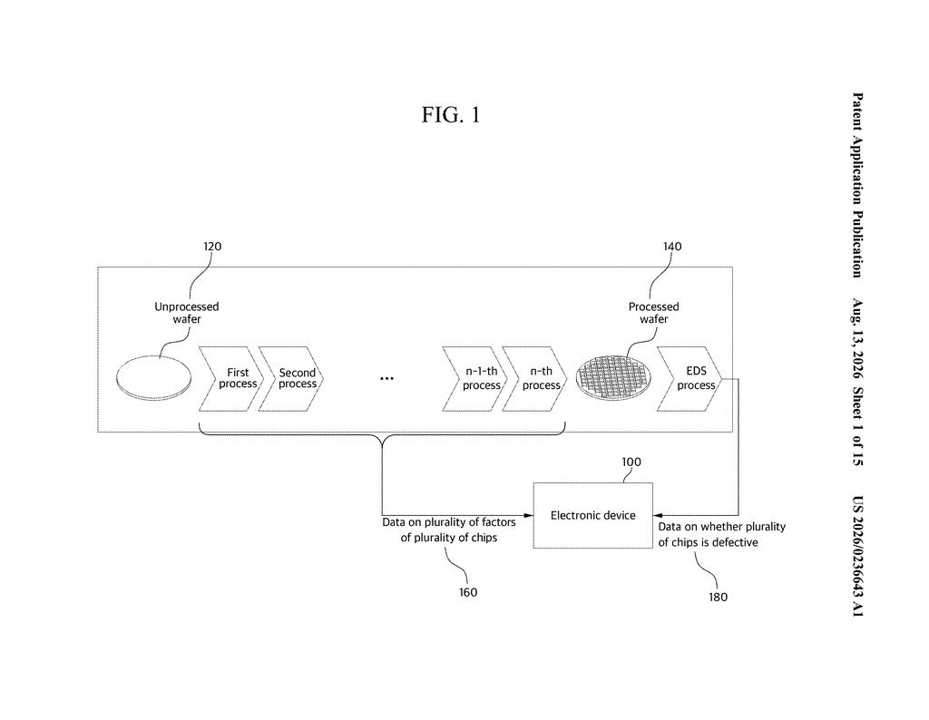
How Samsung's wafer-zone AI spots chip defects early
A chip factory runs the same quality check on every part of a silicon wafer, even though the center and the edges tend to fail for completely different reasons. That kind of uniform inspection misses patterns hiding in the data.
Samsung's patent describes a system that splits a wafer into zones, then trains a separate AI model for each zone using only the measurements most relevant to that specific area. Instead of one broad model trying to cover every corner of the wafer, you get a team of specialized models, each tuned to its own patch of silicon.
The practical goal is better yield prediction, meaning fewer defective chips slipping through to the end of the line, and faster feedback when something in the fabrication process starts going wrong in a particular part of the wafer.
… generating a first sub-data set corresponding to a first area among a plurality of areas in the wafer by dividing the data set based on location data corresponding to each of the plurality of chips …
Translation: The system splits up the wafer data by chip location to analyze specific zones.
How the system builds a separate model for each wafer zone
The system starts by collecting a data set of fabrication factors (think: temperature readings, deposition thickness, etch rates, and similar process measurements) for every chip on a wafer, along with each chip's physical location.
It then divides that data by location, creating a sub-data set for each defined area of the wafer. For each zone, the system runs a selection step: it filters the full list of measured factors down to only those that meet a set condition for that specific area. The claim language says "one or more factors satisfying a condition" without spelling out the condition type, which means the selection logic could be correlation-based, variance-based, or something else Samsung implements internally.
Once the relevant factors are identified for a zone, the system trains an estimation model on that zone's filtered data. In machine-learning terms, this is a form of localized feature selection followed by localized model training, the idea being that the predictors of failure in the wafer's center may be entirely different from those at its edge.
- Acquire full wafer data set with location tags
- Split data by wafer zone
- Select the factors that matter for each zone
- Train a dedicated model per zone
… learning a first estimation model corresponding the first area based on a second sub-data set for the one or more factors of a chip included in the first area.
Translation: It trains an artificial intelligence model tailored specifically to detect defects in that zone.
What this means for chip yield and manufacturing costs
Chip manufacturing yield (the share of working chips per wafer) is one of the biggest cost levers in the semiconductor industry. A system that can predict quality problems earlier, and do so with more geographic precision, could save meaningful money per wafer run, especially at the volumes Samsung's foundry business operates at.
The claim as written is fairly broad: it covers any processor-implemented method that divides wafer data by location, filters factors by condition, and trains a zone-specific model, without requiring a specific algorithm, condition type, or chip geometry. That breadth means the patent, if granted, could put a fence around a wide class of location-aware wafer AI approaches. Samsung's move here sits alongside a wave of new Big Tech patents targeting AI-driven quality control in semiconductor fabrication, a quiet but high-stakes front in the competition to make chips more reliably and cheaply.
Claim 1 is written at a high level of abstraction: it does not lock in a specific algorithm, a specific condition for factor selection, or even a specific number of zones. That breadth is strategically useful for Samsung because it captures the general method of training per-zone wafer models rather than one particular implementation. If granted as written, it could complicate similar AI-based wafer inspection work by competitors without requiring Samsung to have invented a specific formula. The practical risk for rivals is less about this exact technique and more about the wide corridor the claim tries to reserve.
There are more where this came from
We read every patent application Big Tech publishes and send you the ones worth knowing. Plain English, free, every week.
The drawings
15 drawing sheets from US 2026/0236643 A1 · click any drawing to enlarge


Want this weekly breakdown for a company we don't cover? Patentlyze Pro →
Be the first to weigh in