
Samsung
Samsung · Camera · Filed May 14, 2025 · USPTO published Nov 19, 2026 · This week's release
Samsung Patents a Camera Sensor Fix for Faint Stripes in Dark Photos
Zoom in on a photo taken in a dim room and you may spot a faint bright line running straight down the picture. Samsung's patent targets that flaw by changing a tiny reference level inside the sensor, row by row, so the error stops lining up into a stripe.
- Publication number
- US 2026/0370975 A1(US20260370975A1)
- Applicant
- SAMSUNG ELECTRONICS CO., LTD.
- Filed · Published
- May 14, 2025 · Nov 19, 2026
- Inventors
- Jaejin JUNG, Sungyong Kim, Sinhwan Lim
- Status when we published
- Approved; patent expected soon
- Document
- 20 claims
- US classification
- 348/308
- Examiner
- CAMARGO, MARLY S.B. (Art Unit 2638)
What Samsung's camera sensor does about stripes
You take a photo in a dim room, and when you zoom in, a faint bright line runs straight down the picture. Nothing in the scene caused it. The sensor did.
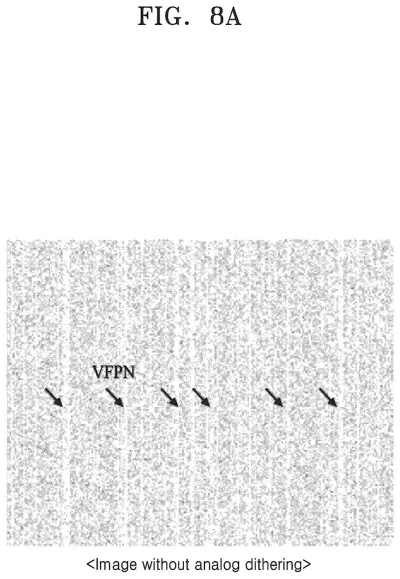
The cause is rounding. Each column of pixels has its own small converter that turns light into a number, and no two converters are perfectly alike. In the dark, one column can land a single step off every time, and a whole line of pixels comes out slightly brighter than its neighbors.
Samsung's fix is to nudge the sensor's internal measuring stick by a tiny, different amount for each row of pixels. The rounding mistakes then scatter into random grain, which is far harder to spot than a straight line. The nudges are balanced so they cancel out and your photo's overall brightness stays put.
… a ramp signal generator configured to generate a ramp signal and adjust an offset of the ramp signal at each read-out period of the pixel array; …
Translation: The chip alters a reference signal during every reading cycle to block fixed pattern noise.
How the sensor shifts its reference row by row
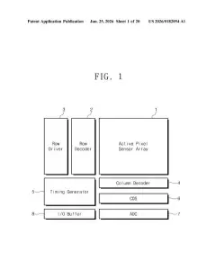
A camera sensor reads its pixels one row at a time. For each pixel, a circuit compares the pixel's voltage with a ramp signal (a reference voltage that falls at a steady rate) and counts clock ticks until the two match. That count becomes the pixel's digital brightness value.
Because the count is a whole number, small timing differences between columns can push one column a single step off. In dark scenes that shows up as vertical fixed pattern noise, a brighter vertical line in the image. The patent's answer is analog dithering (adding a small deliberate wobble so rounding errors scatter randomly). The ramp generator adds an offset, a small shift in the ramp's starting level, and changes it for every row. The slope of the ramp stays the same, and the same offset is applied to both readings the sensor takes of each pixel, so it cancels out of the final value.
The filing describes several details:
- Offsets come from extra current cells that are switched on or off per row, and can be smaller than the sensor's smallest counting step (the example is 0.1 of a step).
- Offsets add up to zero across a frame, and the same row gets the same offset in every frame, which avoids horizontal noise.
- Odd and even columns can get offsets of equal size and opposite sign.
- Dithering runs only when the analog gain (the sensor's amplification setting) is at or below a set value.
… compare each of the plurality of pixel signals with the ramp signal to obtain a plurality of comparison results, and perform analog-to-digital conversion on the plurality of comparison results …
Translation: The system measures incoming light against the moving reference wave to translate visual data into digital photos.
Why cleaner dark photos matter for Samsung phones
The practical payoff is fewer visible stripes in dark shots, and it comes from the sensor itself, with no extra editing step on your phone. The filing lists smartphones, cameras, drones, car driver-assistance systems and home appliances as places this sensor could go, so the fix applies wherever low-light images matter.
On status: this application has been approved, and Samsung has paid the fee to have it issued, so it should become a granted patent soon. It is a narrow, chip-level change. You would notice it only as cleaner dark images.
One more thing to know: the patent office has already approved this application, and Samsung has paid the fee to have it issued, so it should become a granted patent soon. The final granted claims may read a little differently from the version described here.
That makes this Samsung's 170th filing we've tracked since May in our camera sensor push, adding to work like fixing dark photo colors and restoring blurry detail.
Source: US 2026/0370975 A1 at the USPTO (PDF). Full patent text and figures are in the official publication.
Get our take in your Top Stories
Liked this breakdown? Add Patentlyze as a preferred source on Google, and our plain-English take shows up more often in your Top Stories the next time Samsung patent news breaks.
Add Patentlyze on Google
One click.
There are more where this came from
We read every patent application Big Tech publishes and send you the ones worth knowing. Plain English, free, every week.
The drawings · 22 sheets
22 drawing sheets from US 2026/0370975 A1 · click any drawing to enlarge


Show the other 14 sheets


More from Samsung
All 1,662 Samsung patents →
More in Camera
All 271 Camera patents →
Samsung
Samsung Patents a Camera Sensor That Fixes Motion Blur by Counting Individual Light Particles
Samsung
Samsung Patents a Camera Color Fix That Reads the Time of Day
Samsung
Samsung Patents a Refrigerator Camera That Reads the Room Before You Open the Door
Samsung
No comments yet