
Samsung Patents a Camera Chip That Stores More Charge to Capture Cleaner Photos
Samsung is trying to pack more electrical storage directly into the wiring layer of a camera sensor chip, which could reduce noise and save space without adding a separate component.
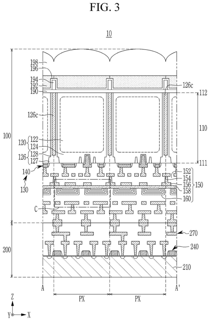
What Samsung's built-in camera capacitor actually does
Every time you open your camera app and tap the shutter, your phone's image sensor is converting light into electrical signals thousands of times per second. That process needs clean, stable electricity, and even tiny fluctuations can show up as noise in your photos.
Samsung's patent describes a way to build a small electrical reservoir, called a capacitor, right into the wiring that already sits on top of the camera chip. Instead of placing that component somewhere else on the circuit board, it lives inside the sensor itself. The design uses multiple thin electrode layers stacked on top of each other, including along the sides, to squeeze more storage capacity into a very small area.
The practical idea is that the sensor can draw on that local charge when it needs it, rather than reaching further across the chip. That shorter distance can mean less electrical interference, which is one of the things that makes a photo look grainy or washed out in low light.
… the wiring portion including a capacitor, the capacitor including a plurality of electrodes and an insulation layer between the plurality of electrodes, wherein the plurality of electrodes include a first electrode group and a second electrode group …
Translation: The sensor uses a specialized capacitor built from multiple layers of electrodes to help manage the electrical charge.
How the stacked electrode layers fit inside the sensor wiring
The patent covers an image sensor made up of three main parts: a substrate (the silicon base), a grid of pixel regions sitting inside and on top of it, and a wiring portion connecting everything together.
Each pixel region contains a photodiode (the part that actually detects light) buried in the silicon, plus a pixel circuit on the surface that reads and amplifies the signal. The wiring layer above that surface is where Samsung is proposing to embed the capacitor.
The capacitor itself is built from multiple thin metal electrode layers separated by insulating material. Crucially, the electrodes are split into two groups that are electrically isolated from each other. The patent's key structural detail is what it calls a side overlap portion: the two electrode groups don't just stack vertically, they also overlap at the sides of the capacitor structure. This sideways overlap adds extra surface area where the two groups face each other across the insulator, which increases how much charge the capacitor can hold without making it physically taller.
In simpler terms, the design gets more storage out of the same footprint by using the side walls of the component, not just the flat top and bottom faces.
The capacitor includes a side overlap portion in which the first electrode group and the second electrode group are stacked at a side surface of the capacitor.
Translation: The chip design stacks the capacitor's internal components along its side to fit more storage capacity into a small space.
What this means for future Samsung camera chip design
Camera sensor chips are under constant pressure to do more in less space. Phones are getting thinner, sensors are getting larger pixel counts, and engineers are always looking for ways to cut down on electrical noise, which is one of the biggest enemies of photo quality in dim conditions. Integrating a high-capacity capacitor directly into the sensor's wiring layer removes the need for a separate decoupling component elsewhere, and the shorter electrical path between the capacitor and the pixel circuits could help stabilize the voltage that each pixel sees.
The claim is narrow enough to be specific, covering a particular geometry (the side overlap) rather than any capacitor inside any sensor, but broad enough to be meaningful if Samsung ships chips with this structure. Filings like this one sit alongside a steady flow of interesting tech patents in the image-sensor and chip-packaging space, where incremental structural improvements often end up in mass-market phone hardware within a few product cycles.
This is the 100th Samsung filing we've tracked since May in our camera sensor push watchlist, adding to work like one showing split zoom views and one mapping photo subjects with AI.
Claim 1 protects a specific physical shape: a capacitor built into the wiring layers of an image sensor, where two groups of electrodes overlap each other along their side surfaces, not just across their faces. That edge-to-edge contact is written directly into the claim, making the protected geometry concrete and testable.
If granted, this blocks anyone from using that same structural arrangement to pack more storage capacity into the wiring of an image sensor. The practical target is clear: chips with millions of pixels crammed into a space smaller than a fingernail, where squeezing extra charge storage out of every layer matters for image quality.
The claim is narrow enough to have a real boundary and broad enough to cover a genuine manufacturing decision. A patent on a specific geometry is a patent on something you either build or you don't, and that makes it enforceable in ways that matter.
Get our take in your Top Stories
Liked this breakdown? Add Patentlyze as a preferred source on Google, and our plain-English take shows up more often in your Top Stories the next time Samsung patent news breaks.
There are more where this came from
We read every patent application Big Tech publishes and send you the ones worth knowing. Plain English, free, every week.
The drawings
15 drawing sheets from US 2026/0255715 A1 · click any drawing to enlarge


Want this weekly breakdown for a company we don't cover? Patentlyze Pro →
Be the first to weigh in