
AMD Patents Chip Design That Keeps AI Calculations Accurate Without Wasting Silicon
AMD is patenting a chip-level trick that lets different clusters of math hardware use their own separate scaling numbers, a change that could make AI matrix operations more accurate without blowing out chip area.
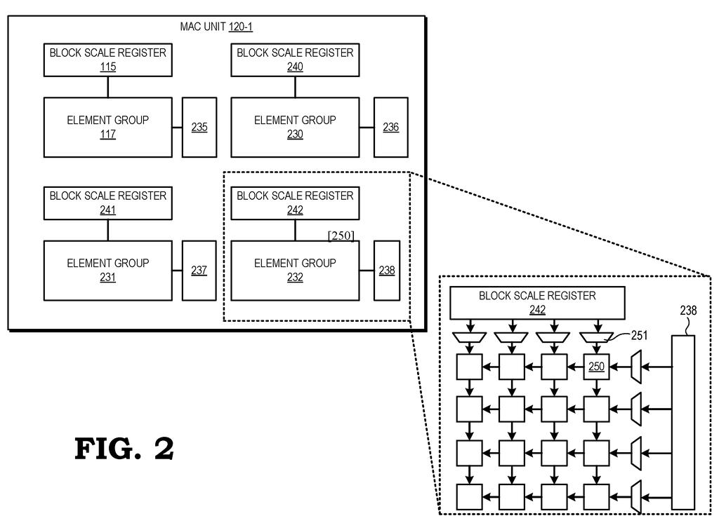
What AMD's block scale register design actually does
Imagine your calculator had to apply a different unit conversion to every single column of a massive spreadsheet, but it only had one conversion dial shared across the whole thing. Everything either gets rounded into the same bucket or the chip has to do expensive extra work to sort it all out.
That's roughly the problem AMD is solving here. When a chip does the kind of heavy math that powers AI models, numbers at very different scales have to be multiplied together. AMD's patent describes a design where each cluster of math units gets its own dedicated "scale register" so it can apply the right scaling factor for its piece of the problem independently.
The result is that the chip can handle mixed-precision matrix math (multiplying matrices where the numbers span very different ranges) more efficiently. Instead of one shared approach that wastes either accuracy or chip space, each group of arithmetic units gets exactly the data it needs.
… a first block scale register configured to provide a first scale factor to the first element group and a second block scale register configured to provide a second scale factor to the second element group.
Translation: Separate memory registers feed different adjustment values to distinct blocks of math circuits.
How separate registers deliver scale factors to each math group
The patent describes a matrix arithmetic unit inside a processor that is divided into multiple arithmetic element groups. Think of each group as a small team of multipliers working in parallel on a slice of a larger matrix calculation.
Each group is paired with its own block scale register, a tiny dedicated storage cell that holds a scale factor (essentially a number that tells the math units how to rescale their inputs before or during the multiplication). The first group reads from the first block scale register; the second group reads from the second, and so on.
- Scale factors applied early: The arithmetic elements apply the scale data to their operands before or during the matrix operation, so downstream results are already in the right numeric range.
- Outer product operations: The patent specifically calls out outer product operations (a type of matrix multiply used heavily in neural network layers) as a target workload.
- Area efficiency: By scoping each register to one group rather than broadcasting one global register everywhere, the design avoids the extra wiring and logic that a fully flexible scheme would require.
The key engineering trade-off the patent is navigating is between flexibility (every element gets its own scale) and area (registers and routing consume silicon). Block-level granularity sits in the middle: coarse enough to keep the circuit small, fine enough to handle the scaling variation that real AI workloads produce.
By employing block scale registers to provide the scale data to the groups of arithmetic elements, the processor is able to efficiently implement scale operations without consuming an undesirably large amount of circuit area.
Translation: Using dedicated scale registers lets the chip handle accuracy adjustments without wasting valuable physical space on the silicon.
What this means for AMD's AI chip efficiency
For AMD, this matters most in the context of low-precision AI inference. Techniques like FP8 and microscaling formats (used in AI training and inference to squeeze more operations per watt) require exactly this kind of per-group scaling to stay accurate. Without dedicated scale registers at the hardware level, a chip either loses precision or burns extra cycles applying corrections in software.
The patent's emphasis on keeping circuit area small is a telling detail. AI chips are already enormous and expensive to manufacture, so any design that delivers a capability without proportionally growing the die is worth filing. AMD's work on AI accelerators and its CDNA and RDNA GPU architectures are the obvious homes for this kind of hardware feature, and chip-level matrix scaling is one of the areas covered in this week's Big Tech patents across the semiconductor space.
AMD's 32nd filing we've tracked since May in our AI chip wars watch builds on splitting AI work across chips and faster on-chip data conversion.
Block scale registers are established hardware. AMD already builds the matrix units described in this patent.
The patent focuses specifically on saving chip space, which means the engineers have already done the math that usually comes just before a real build decision. The underlying structure this feature would plug into already exists in chips you can buy today.
That mix of ready infrastructure and documented area analysis puts this closer to a shipping product than most hardware patents ever get.
Get our take in your Top Stories
Liked this breakdown? Add Patentlyze as a preferred source on Google, and our plain-English take shows up more often in your Top Stories the next time AMD patent news breaks.
There are more where this came from
We read every patent application Big Tech publishes and send you the ones worth knowing. Plain English, free, every week.
The drawings
7 drawing sheets from US 2026/0244705 A1 · click any drawing to enlarge


Want this weekly breakdown for a company we don't cover? Patentlyze Pro →
Be the first to weigh in