
Samsung Files Patent to Shrink Display Pixels for AR Glasses
Each dot on a micro-LED screen needs bulky, high-voltage electronics, and that bulk limits how sharp a tiny display can get. Samsung's filing cuts that bulk down to a single part per pixel.
What Samsung's memory-in-every-pixel display does
The light behind each dot on a micro-LED screen needs a fairly high voltage to glow. The transistors (tiny electronic switches) built to handle that voltage take up more room than ordinary ones. That's a problem when you want a very sharp picture on something as small as a pair of AR glasses, where every sliver of space counts.
Samsung's filing rearranges the circuitry inside each pixel. Only one transistor, the one that feeds power straight to the light, is built for high voltage. Everything else, including a few bits of memory that remember how bright the pixel should be, runs on low voltage and can be much smaller.
The space saved goes to that memory, which can hold data for several slices of a single frame. The shared settings that tell each pixel how much current to use come from a circuit outside the pixel, which keeps the pixels themselves lean.
Separation of the control circuit and the current source transistor enables reduced high-voltage transistor usage and improved pixel integration.
Translation: Splitting these parts allows the screens to use lower voltage and pack pixels closer together.
How one high-voltage part per pixel saves space
Every pixel has a micro-LED (a light-emitting diode only a few microns to tens of microns across). Brightness is set with pulse width modulation, or PWM (flicking the light on and off very fast, where the share of time it spends on sets how bright it looks). In the filing's example, an 8-bit brightness value is split into eight slices of each frame, each a different length. The pixel's own memory (latches, flip-flops or SRAM) stores the bits and turns the light on for the slices marked 1.
The pixel is split into four jobs:
- Control circuit: memory devices store the brightness bits and output the PWM signal.
- Control transistor: the PWM signal opens and closes it, passing the supply voltage to the driving circuit.
- Driving circuit: a current source transistor, the only high-voltage part, sets how much current reaches the micro-LED.
- Bias circuit: sits outside the pixels and sends shared reference voltages along each row.
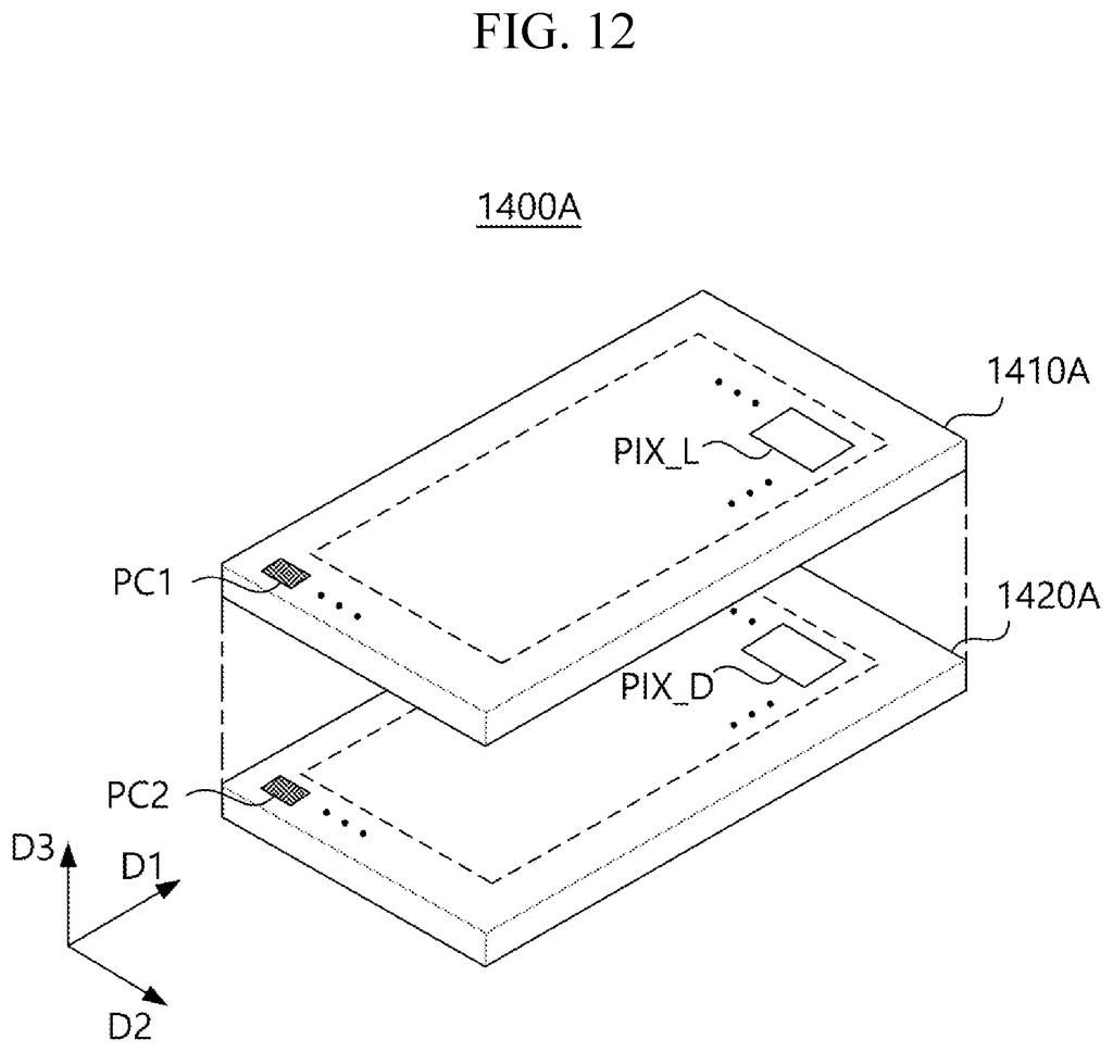
The filing also describes variations. A pixel can have several current paths with switches, each controlled by a tiny memory, to even out brightness differences between individual LEDs. Another version uses a multiplexer (a selector switch) to pick one of several bias voltages. The screen can be built as two stacked layers joined by hybrid copper bonding, and one claim adds an optical waveguide (a glass or polymer channel) that guides the light to a see-through display area.
Why this matters for thin AR glasses displays
If you ever wear AR glasses, the screen has to be tiny, sharp and still readable against the real world. Micro-LEDs are attractive for that because they can be bright and fast. Their high-voltage electronics make each pixel bigger, though, which caps how sharp a small display can get. Shrinking the number of bulky parts attacks that limit directly.
The filing is about the circuit inside the pixel, so it applies to any small, high-resolution display that uses micro-LEDs. It names AR glasses as its target. It's a patent application, so it doesn't tell you whether Samsung will ship a screen built this way.
Samsung's 68th filing we've tracked since May in the AR glasses race builds on earlier applications like darkening backdrops in AR and fading real objects into VR.
The problem is real. A display for glasses has to be tiny and sharp at once, and every transistor in a pixel eats space that could hold more pixels. High-voltage parts are the biggest space hogs, so cutting them to one per pixel goes straight at the bottleneck.
The approach is a reshuffle of the circuit inside each pixel, a modest change matched to a narrow problem. The filing gives no numbers for how much smaller a pixel gets, so the size of the win is unknown.
For you, any payoff would show up indirectly: sharper displays in smaller packages, if they ever reach a product. It's an engineering fix for one stubborn limit, and it looks sensible on paper.
Get our take in your Top Stories
Liked this breakdown? Add Patentlyze as a preferred source on Google, and our plain-English take shows up more often in your Top Stories the next time Samsung patent news breaks.
There are more where this came from
We read every patent application Big Tech publishes and send you the ones worth knowing. Plain English, free, every week.
The drawings
12 drawing sheets from US 2026/0331035 A1 · click any drawing to enlarge


Show the other 4 sheets


Want this weekly breakdown for a company we don't cover? Patentlyze Pro →
Be the first to weigh in