
Samsung Patents a Shorter Signal Path Inside Stacked Camera Chips
Samsung has filed a patent for a new wiring layout inside image sensors that cuts the distance electrical signals travel between the two chips stacked inside a modern camera module. Shorter paths mean less noise and potentially sharper photos.
What Samsung's stacked image sensor wiring actually does
Modern smartphone cameras already pack two separate chips on top of each other inside a single image sensor. The problem is connecting them: getting an electrical signal from one chip to the other requires routing it through several layers of material, and every extra hop can add noise or slow things down.
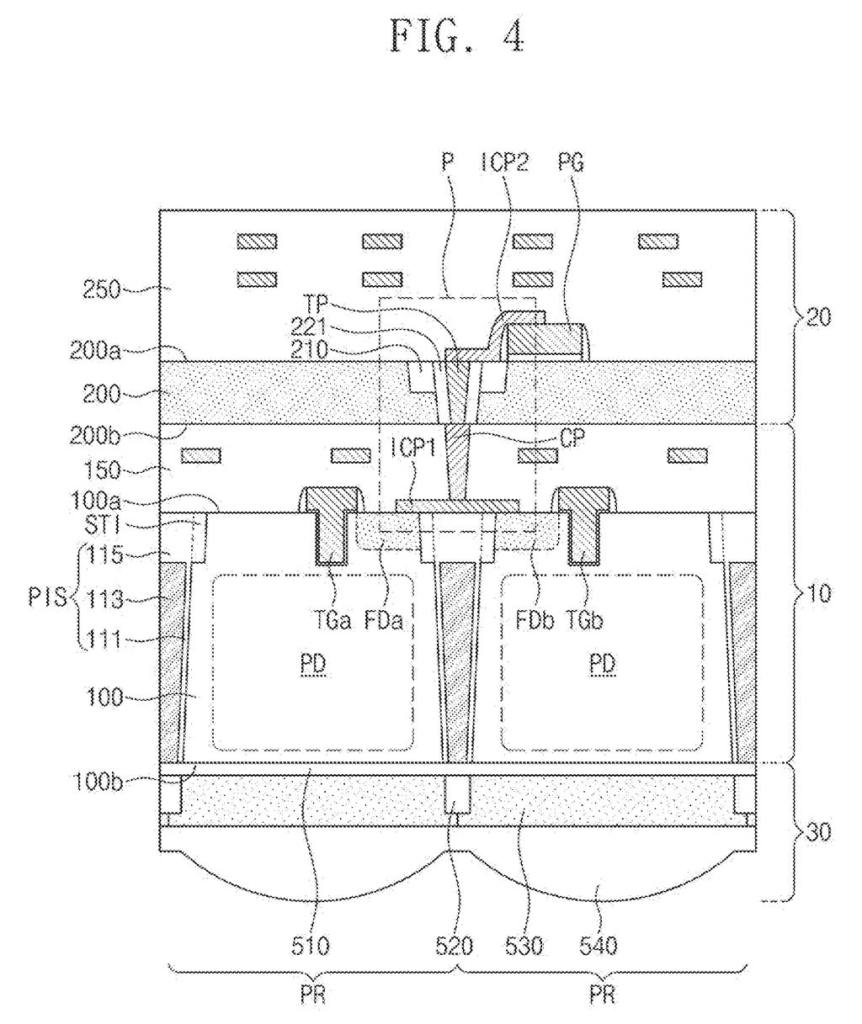
Samsung's patent describes a more direct path. A plug-like conductor punches straight through the top chip and links directly to a circuit on the bottom chip that catches the light. Then a short metal connector on the top chip ties that plug to the transistor that reads the signal. The result is a tighter, more direct handoff between the two chips.
For you, this kind of engineering is invisible but its effects are not. A cleaner signal path can mean less visual noise in low-light photos, finer detail in fast-moving scenes, and a sensor that uses a bit less power to do its job.
… a contact plug between the first semiconductor substrate and the second semiconductor substrate, and connected with the floating diffusion region; a through plug penetrating through the second semiconductor substrate and connected with the contact plug …
Translation: The design uses a series of vertical metal connectors to bridge the gap between the two stacked layers of the camera chip.
How the through-plug routes signals across two substrates
The patent describes an image sensor built from two semiconductor substrates (essentially two chips) stacked one on top of the other. The bottom chip holds the floating diffusion region, the area that collects the tiny electrical charge produced when light hits a pixel and converts it into a voltage.
Connecting that charge-collection zone to the readout circuitry on the top chip is the core engineering challenge here. Samsung's solution involves three pieces:
- A contact plug sitting between the two chips, touching the floating diffusion region on the bottom chip.
- A through plug that passes vertically all the way through the top chip, like a nail driven through a board, connecting to the contact plug below.
- An upper connection pattern, a short metal trace on the surface of the top chip, that links the through plug to the pixel transistor (the circuit that actually reads and amplifies the signal).
The key detail the patent emphasizes is that the upper connection pattern touches the first surface of the through plug, meaning the handoff happens at the very top of that vertical conductor rather than somewhere mid-layer. That precision matters because it controls where electrical resistance (and therefore noise) enters the signal chain.
… an upper connection pattern connecting the through plug with the pixel transistor on the second semiconductor substrate, wherein the upper connection pattern contacts a first surface of the through plug.
Translation: A specialized metal path links the internal wiring to the transistor on the top layer to shorten the signal distance.
What this means for phone camera image quality
For anyone who has ever zoomed into a low-light photo and seen a grainy, speckled mess, this kind of patent is about the wiring inside the sensor that contributes to that problem. Shorter, more direct signal paths between stacked chips reduce the chances that the tiny electrical charge from each pixel gets corrupted before it can be read. That translates to cleaner images, particularly at night or in fast-action scenes where cameras are already working at the edge of their sensitivity.
Samsung supplies image sensors to a wide range of phone makers, so improvements at this chip-architecture level can ripple across many devices. The stacked-sensor design this patent refines is already the standard in flagship cameras, and each incremental improvement in how layers connect is part of how camera hardware keeps getting better without the sensors physically growing larger. Filings like this one sit alongside the plain-English patent summaries covering the broader push by chip companies to squeeze more image fidelity out of the same physical footprint.
That makes this Samsung's 97th filing we've tracked since May in our camera sensor push, adding to work like the folded zoom design and the charge-storage sensor.
You will not open a box one day and notice that the wiring inside your camera chip got tidier. What you might notice, across a couple of phone upgrades, is that photos taken in dim restaurants or at dusk look cleaner without the chip itself getting any larger. The reason is simple: shorter, more precisely connected paths inside the sensor mean the electrical signal from each tiny light-catching cell reaches the processing layer with less interference.
Less interference means less of that speckled, washed-out noise that ruins low-light shots. Samsung is essentially patenting the exact point where two internal conductors meet, which tells you the engineering here is about precision at a scale invisible to everyone except the people designing the chip.
That discipline is what separates a camera that struggles at night from one that does not.
Get our take in your Top Stories
Liked this breakdown? Add Patentlyze as a preferred source on Google, and our plain-English take shows up more often in your Top Stories the next time Samsung patent news breaks.
There are more where this came from
We read every patent application Big Tech publishes and send you the ones worth knowing. Plain English, free, every week.
The drawings
23 drawing sheets from US 2026/0255716 A1 · click any drawing to enlarge


Want this weekly breakdown for a company we don't cover? Patentlyze Pro →
Be the first to weigh in