
Samsung's New Patent Stops Its Screen Pixels and Light Sensors from Tripping Over Each Other
Cramming light sensors directly into a display panel sounds simple, but the pixels and sensors end up fighting over the same timing signals. Samsung's new patent describes a way to give each side its own schedule so they stop interfering with each other.
What Samsung's in-screen sensor timing fix actually does
Imagine your phone's screen is trying to both show you a picture and take a picture at the exact same moment. The electronics that drive the glowing pixels and the electronics that read incoming light share the same grid of wires, and if they fire at the same instant, they can scramble each other's results.
Samsung's patent tackles this by making the light-emitting side and the light-sensing side of the display operate on slightly different clocks, even when they sit on the same physical row of the screen. Think of it like a traffic light that gives pedestrians and cars a small gap between their green lights so they never fully overlap.
The practical payoff is a display that can embed sensors (for fingerprints, cameras, or health tracking) directly behind the screen without the pixels drowning out the sensor readings. You get a cleaner, flatter device without a separate sensor cutout or notch.
How the circuit rows stagger their scan signal timing
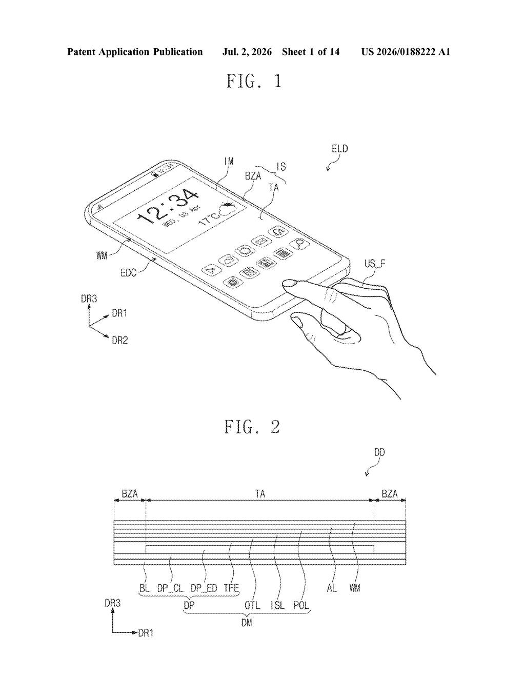
The display is built in three layers: a base layer at the bottom, a circuit layer in the middle, and an element layer on top. The element layer holds two types of components: light emitting elements (the pixels that produce the image) and light receiving elements (sensors that detect incoming light, like a fingerprint or ambient-light sensor).
Both types of elements are wired to circuits in the middle layer. Normally, circuits in the same physical row of a display receive the same scan signal (a timed electrical pulse that tells each row when to activate). The problem is that pixel circuits and sensor circuits need very different things from that signal: pixels want to light up, while sensors want quiet time to detect reflected light without the pixels' own glow getting in the way.
Samsung's approach assigns each row a different transition time point for its pixel scan signal versus its sensor scan signal. In plain terms, the pixel in row one turns on at time A, and the sensor in the same row turns on at time B, where A and B don't overlap.
This staggered schedule means:
- The sensor captures light during a window when the adjacent pixels are not actively changing state.
- Electrical noise from pixel switching doesn't corrupt the sensor reading.
- Both functions share the same physical grid without requiring extra rows of circuitry or a separate sensor panel.
What this means for under-display cameras and fingerprint sensors
Under-display fingerprint readers exist today, but they typically rely on specific zones of the screen and careful partitioning. This patent points toward a more generalized approach where any row of the display can host a sensor alongside its pixels, which would make it much easier to spread sensors across the full panel area. That's the prerequisite for things like a camera hidden behind the entire screen or health sensors distributed across a large display.
For you as a user, the near-term implication is cleaner device designs: no punch-hole camera, no sensor bar, no notch. The longer-term implication is displays that double as sensing surfaces across their full area, opening the door to features like on-screen health monitoring without any visible hardware cutouts.
This is genuinely useful foundational work. Staggering scan-signal timing sounds like a small tweak, but it's exactly the kind of low-level circuit design that determines whether full-panel under-display sensors are practical or just a demo-booth trick. Samsung Display filing this suggests the company is actively engineering toward a notch-free, sensor-embedded display at scale, not just talking about it.
Get our take in your Top Stories
Liked this breakdown? Add Patentlyze as a preferred source on Google, and our plain-English take shows up more often in your Top Stories the next time Samsung patent news breaks.
There are more where this came from
We read every patent application Big Tech publishes and send you the ones worth knowing. Plain English, free, every week.
Want this weekly breakdown for a company we don't cover? Patentlyze Pro →