
Sony Patents a Camera Chip That Sharpens Detail in Dim or Fast-Moving Shots
Sony has patented a way to make image sensors work more efficiently by letting the chip dial its own precision up or down depending on how long each pixel is exposed to light, a trick that could shrink chip circuits without sacrificing image quality.
What Sony's adaptive image sensor resolution actually does
You're shooting a photo in a high-contrast scene: part of the frame is blazing sunlight, part is deep shadow. To capture both, your camera takes multiple exposures in rapid succession, one very short, one longer. Each of those exposures needs to be converted from raw light data into numbers the camera can process.
The problem is that each exposure doesn't need the same level of numeric detail. A very short exposure captures a narrow range of brightness, so you don't need as many decimal places to describe it accurately. Sony's patent lets the chip recognize this and automatically reduce its precision for short exposures, then dial it back up for longer ones.
The payoff is a smaller, more efficient chip. Less circuitry means less power use, lower heat, and potentially lower cost, without losing any image quality you'd actually notice.
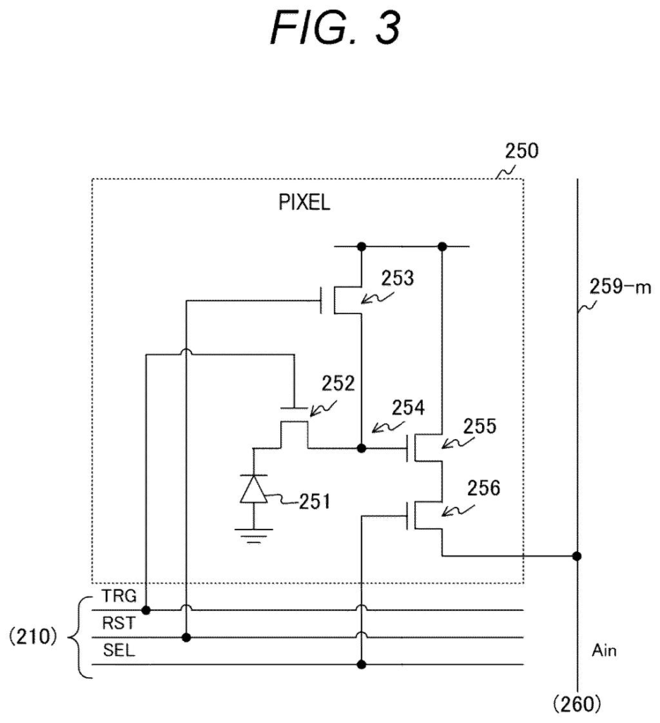
a pixel that sequentially generates a plurality of analog signals having different exposure times; an analog-to-digital converter that sequentially converts each of the plurality of analog signals into a digital signal; and a logic circuit that controls resolution of the analog-to-digital converter according to an exposure time.
Translation: The sensor captures multiple images at different speeds and adjusts its digital processing to match each one.
How the logic circuit shifts AD converter resolution per exposure
At the heart of every digital camera sensor is an analog-to-digital (AD) converter, which translates raw electrical signals from pixels into binary numbers a processor can work with. The more bits the converter uses, the finer its precision (called resolution in this context), and the more circuitry it requires.
Sony's patent describes a sensor that captures multiple exposures per frame, each with a different shutter duration. This is the standard approach for HDR (high dynamic range) imaging, where short exposures preserve highlight detail and long exposures reveal shadow detail.
The new element is a logic circuit that watches the exposure time and tells the AD converter how much resolution it actually needs for each shot:
- Short exposures carry a compressed brightness range, so the converter operates at lower bit depth.
- Long exposures carry a wider range, so the converter shifts to higher bit depth.
- The logic circuit manages this switching automatically, frame by frame.
This variable-resolution approach means the chip does not need to be sized for worst-case precision at all times. The claim is a measurable reduction in circuit scale, the physical transistor count and wiring that determines how large and power-hungry the chip is.
Suppression of circuit scale increases in a solid-state imaging element that performs AD conversion is disclosed.
Translation: Sony designed this technology to keep the camera hardware small while still handling complex image processing.
What this means for HDR camera chips in phones and cameras
HDR imaging is now a baseline expectation in smartphones and mirrorless cameras, but fitting the supporting circuitry onto an increasingly compact sensor stack is a genuine engineering headache. Every extra transistor costs area, power, and heat budget. Sony's approach attacks that cost at the AD converter level, which is one of the more power-hungry subsystems on a sensor chip.
Sony Semiconductor Solutions is the supplier behind image sensors in a wide range of devices, from iPhones to PlayStation cameras to automotive systems. A circuit-scale reduction in their core sensor architecture would ripple across all of those product lines. For a broader look at where imaging and chip design intersect with intellectual property, Sony's filing sits alongside this week's Big Tech patents covering the full range of semiconductor innovation.
The problem here is real and measurable: HDR sensors need multiple conversion cycles per frame, and sizing the AD converter for full precision on every cycle is wasteful. Sony's solution is proportionate and architecturally clean, matching converter precision to the information content of each exposure rather than over-engineering the hardware. Whether the circuit savings are large enough to matter at the product level depends on implementation details the patent does not fully reveal, but the underlying logic is sound and fits a genuine cost pressure in sensor design.
There are more where this came from
We read every patent application Big Tech publishes and send you the ones worth knowing. Plain English, free, every week.
The drawings
38 drawing sheets from US 2026/0238900 A1 · click any drawing to enlarge


Want this weekly breakdown for a company we don't cover? Patentlyze Pro →
Be the first to weigh in