
Sony Patent Lets Shared Camera Pixels Keep Individual Light Sensitivity Controls
Camera sensors cram millions of tiny light-catching pixels into a tight space, and sharing circuitry between them is a common space-saving trick. Sony's new patent finds a way to share that circuitry without giving up each pixel's ability to control exactly how sensitive it is to light.
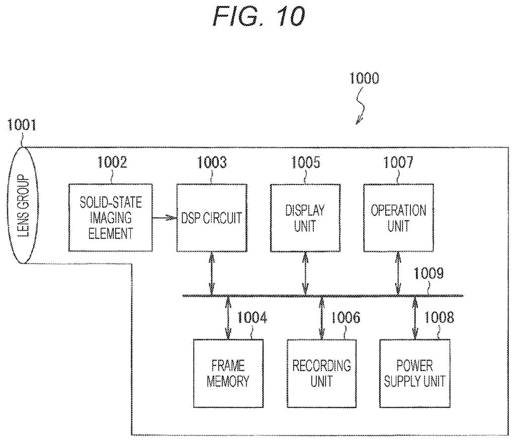
What Sony's per-pixel sensitivity fix actually does
Ever wondered why some phone cameras struggle in low light even though they're packed with millions of pixels? The answer is often in the circuitry behind each pixel, not the pixels themselves.
Camera sensors work by having tiny photo-sensitive spots convert light into an electrical signal. To save space on the chip, manufacturers often share some of the supporting electronics between neighboring pixels. The problem is that sharing too much circuitry can make pixels less sensitive to dim light, and it can throw off the optical balance of the sensor. Sony's patent describes a way to keep one key circuit, a small transistor that controls how well each pixel converts light into a signal, dedicated to each individual pixel, even while other supporting transistors are still shared.
The result is a sensor that gets the space-saving benefits of sharing while keeping each pixel's light-conversion performance as strong as if nothing were shared at all. It's a relatively quiet engineering fix, but in camera design, small wins in sensitivity can mean noticeably better photos in difficult lighting.
… a conversion-efficiency adjustment transistor configured to adjust a conversion efficiency of the signal charge stored in the floating diffusion portion …
Translation: A dedicated part adjusts how efficiently each pixel handles its stored electrical charge.
How the conversion-efficiency transistor wiring works
At the heart of any digital camera sensor is a process called photoelectric conversion: light hits a tiny well (the photoelectric conversion unit), knocks loose an electrical charge, and that charge gets stored in a small capacitor called a floating diffusion. The floating diffusion's voltage is then amplified and read out as the pixel's brightness value.
A critical performance number here is conversion efficiency, basically how large a voltage swing you get per unit of stored charge. Higher conversion efficiency means the sensor can detect fainter light. Sony's patent adds a dedicated conversion-efficiency adjustment transistor to each pixel. By switching this transistor on or off, the sensor can change the effective size of the floating diffusion capacitor, toggling between a high-sensitivity mode (small capacitor, big voltage swing) and a high-dynamic-range mode (larger capacitor, smaller swing that doesn't clip in bright light).
The tricky part is doing this while also sharing circuitry. In a conventional shared-pixel design, several pixels pool a single reset transistor (which clears the floating diffusion between exposures) and a single selection transistor (which routes one pixel's signal to the output line at a time). Sony's patent describes two specific wiring configurations:
- Each pixel keeps its own conversion-efficiency transistor and its own amplifier; only the reset transistor is shared, connected to a wire that runs through all the individual conversion-efficiency transistors.
- Alternatively, each pixel keeps its own conversion-efficiency transistor; the amplifiers are shared, and the selection transistor connects to the wire linking all those amplifiers.
Both arrangements preserve optical symmetry, meaning the pixel layout looks identical from the lens's point of view, which matters for avoiding image artifacts like color shading across the frame.
… enhance the conversion efficiency to a degree similar to that of a non-sharing pixel and can maintain the optical symmetry also in a case where sharing between pixels is performed …
Translation: This design keeps shared pixels performing just as well as individual ones without losing visual balance.
What this means for future Sony camera sensors
For consumers, better conversion efficiency in dim light is the difference between a sharp photo at a dinner table and a blurry, noisy one. Sony supplies image sensors to a wide range of smartphone makers and camera brands, so engineering choices made in a patent like this can show up in tens of millions of devices. Keeping per-pixel sensitivity control intact while still shrinking the transistor count is the kind of incremental gain that accumulates into a meaningfully better camera over successive product generations.
The design does reflect a real tradeoff: sharing transistors at all introduces some constraint on how independently neighboring pixels can be read out, which matters for fast readout speeds needed in video. Sony is betting that the sensitivity and symmetry benefits outweigh that complexity cost. Imaging-chip new tech patents from Sony and its rivals have been clustering around exactly this tension between pixel density, dynamic range, and low-light performance as sensors push toward ever-smaller pixel sizes.
This is the 70th Sony filing we've tracked in our Display coverage since May, a topic that includes one on faster moving subject detection and one on a self-powered image device.
Giving every pixel its own reading circuit recovers light sensitivity, but that gain has to be paid for somewhere. Sony's answer is to have groups of pixels share other circuits, like the one that clears the sensor between shots. That sharing shrinks the chip, but it also means every pixel in a group gets reset at the same instant, which limits how flexibly the camera can sequence its readings.
The deeper cost shows up in image quality. When pixels share the path that amplifies their signal, a faint trace of one pixel's reading can bleed into its neighbor's, producing the subtle banding stripes that make dark restaurant photos look artificially smoothed.
For a phone camera, where capturing something usable in dim light matters far more than precise readout control, the trade reads as worth it. The sensitivity improvement is something a user will see; the downsides are narrow and, in ordinary shooting, nearly invisible.
Get our take in your Top Stories
Liked this breakdown? Add Patentlyze as a preferred source on Google, and our plain-English take shows up more often in your Top Stories the next time Sony patent news breaks.
There are more where this came from
We read every patent application Big Tech publishes and send you the ones worth knowing. Plain English, free, every week.
The drawings
10 drawing sheets from US 2026/0255081 A1 · click any drawing to enlarge


Want this weekly breakdown for a company we don't cover? Patentlyze Pro →
Be the first to weigh in