
Sony Patents a Pixel Design That Reads Light Two Ways at Once
Sony is patenting an image sensor where every pixel simultaneously feeds two separate circuits, potentially allowing a single sensor to capture both fine detail and motion information without choosing between them.
What Sony's dual-readout camera sensor actually does
You're shooting a video in a room where someone keeps flicking the lights, and your phone's camera has to pick: expose for the bright moments or the dark ones, but not both. That tradeoff is baked into how most sensors are built today.
Sony's patent describes a sensor pixel that feeds two separate electronic circuits at the same time. One circuit handles the signal the usual way, and a second circuit runs its own independent read on the same incoming light. Because both readings come from the same physical spot on the sensor, they are perfectly aligned in time and space.
Sony frames this as a hardware-level fix rather than a software trick. Instead of taking two shots and blending them in software, the sensor itself captures two data streams from every pixel in a single exposure.
… a readout circuit configured to output a first signal based on a first photocurrent, the first photocurrent being outputted by the photoelectric conversion layer, and an AD conversion circuit configured to output a second signal based on a second photocurrent …
Translation: The sensor uses two different circuits to process light data simultaneously, creating two separate signals from one layer.
How one pixel layer feeds two separate circuits
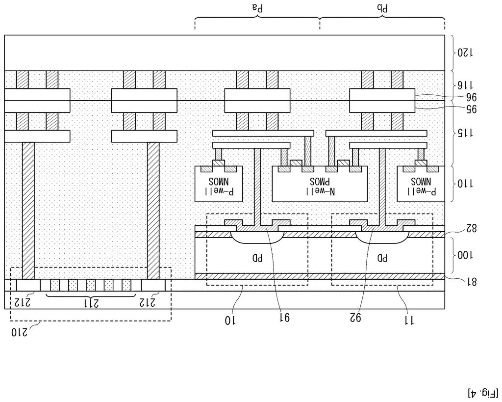
The patent describes a photodetector (the chip that converts light into electrical signals, the core of any camera sensor) built around a specific architecture: each pixel unit contains a photoelectric conversion layer that generates current whenever light hits it.
What makes this design distinct is that the layer's output current is split and routed to two separate downstream circuits inside the same pixel:
- A readout circuit that processes the first portion of the current and produces a conventional analog signal.
- An AD conversion circuit (analog-to-digital converter, the component that turns electrical levels into numbers a processor can use) that processes a second portion of the current and produces a digital signal independently.
Both circuits draw from the same light-gathering layer, so both readings correspond to exactly the same moment and location. The patent does not specify how the two output signals are combined or used downstream, but having two independent data streams from a single pixel opens the door to wider dynamic range, faster readout, or parallel processing pipelines.
The claim covers an array of these dual-output pixel units, suggesting this is designed as a full image sensor, not just a single test pixel.
A photodetector according to an embodiment of the present disclosure includes a plurality of pixel units each including a photoelectric conversion layer configured to output a photocurrent by photoelectric conversion …
Translation: This device is made of many tiny pixel units that turn incoming light into electrical current.
What this means for sensors in phones and cameras
Sony Semiconductor Solutions is one of the world's largest suppliers of image sensors, with its chips inside a huge share of smartphones and cameras. A structural change at the pixel level, if it makes it to production, would filter through to countless devices. The practical benefit most likely to reach consumers is better performance in mixed or rapidly changing lighting, since the sensor would have two independent reads of each pixel rather than one.
This is a foundational chip-architecture filing, and it sits alongside a steady stream of latest Big Tech patents targeting image sensor efficiency and per-pixel data throughput. Whether Sony's dual-circuit approach ends up in a shipping product depends on yield, power budget, and die size tradeoffs that the patent doesn't address.
Sony's 342nd filing among the applications we've tracked since May in our Sony coverage joins earlier work on reading glare to find light and mixing avatars across virtual worlds.
The ship path here is long. Building two functional readout circuits inside a single pixel unit adds complexity to the silicon layout, raises power consumption per pixel, and tightens manufacturing tolerances, none of which the filing addresses. Sony would need to demonstrate that the yield loss from the added circuitry doesn't outweigh the image-quality gain before committing this to a production sensor. The concept is sound, and Sony has the fabrication expertise to pursue it, but this reads like early-stage architecture exploration rather than something six months from a product announcement.
There are more where this came from
We read every patent application Big Tech publishes and send you the ones worth knowing. Plain English, free, every week.
The drawings
15 drawing sheets from US 2026/0247052 A1 · click any drawing to enlarge


Want this weekly breakdown for a company we don't cover? Patentlyze Pro →
Be the first to weigh in