
Samsung Patents a Three-Layer Lens Stack With Offset Fill Points for Displays
Making a multi-layer lens sounds simple enough, but the spot where you inject the lens material during manufacturing can leave a tiny flaw in the finished optic. Samsung's solution: stagger those spots so no two layers line up.
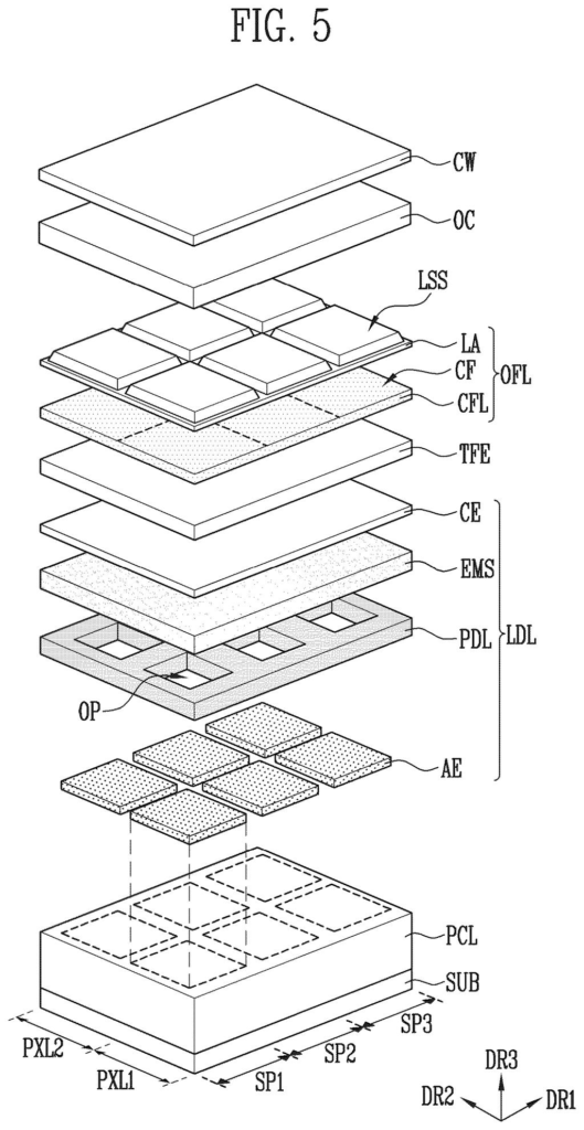
What Samsung's stacked lens design actually does
Imagine stacking three pancakes, but each one has a small seam where the batter was poured in. If all three seams line up in the same spot, you end up with a weak point running straight through the stack. Samsung's patent works around exactly that problem, but for lenses instead of pancakes.
The patent describes a lens assembly made of three separate lens layers, one closest to the incoming light, one in the middle, and one closest to where the light exits. Each layer is made by injecting liquid lens material into a mold, and that injection point leaves a tiny mark called a gate mark. Samsung's key idea is to place each layer's injection point at a different spot around the lens so they never overlap.
The goal is cleaner, more uniform optics. When the injection points are staggered, any small imperfection from the molding process doesn't stack on top of itself and create a visible or performance-affecting flaw. This matters most in compact, high-precision displays like those used in phones or wearable screens.
How the offset injection ports prevent optical defects
The patent covers a three-lens assembly designed for display devices, where light enters from one side (the incident side) and exits the other. Each of the three lenses is formed by injecting liquid polymer into a mold, a common manufacturing technique for plastic optics.
The critical detail is the placement of the material injection part on each lens. Think of this like the gate in injection molding: the spot where material flows in always leaves a small residual mark or stress concentration. The patent specifies that:
- The first lens (closest to the light source) has its injection point at one position.
- The second, middle lens has its injection point at a different angular or radial position.
- The third lens (closest to the exit) has its injection point at yet another distinct position.
When viewed from above in a plan view (looking straight down through the stack), none of the three injection points align with each other. This deliberate offset prevents cumulative optical distortion or structural weakness that would occur if all three gate marks sat directly on top of one another. The patent does not specify exact angular offsets, leaving room for design flexibility across different lens sizes and display form factors.
What this means for Samsung's display and AR hardware
For anyone using a Samsung phone, tablet, or future wearable with a compact display module, lens quality directly affects image sharpness and brightness consistency. Manufacturing defects in stacked optics are a known headache in tight display assemblies, and small gate-mark misalignments can scatter light in ways that show up as halos or dim spots.
This patent is narrow and manufacturing-focused, which means it's the kind of incremental quality improvement that rarely makes headlines but does show up in production yield and display consistency. Samsung Display supplies panels and optical components broadly, so a cleaner lens-stack process could benefit multiple product lines across different device makers, not just Samsung's own branded hardware.
This is a quiet manufacturing patent, not a product reveal. The underlying idea is straightforward: offset your mold gates so defects don't compound. It's genuinely useful engineering, but it's the kind of filing that matters to a process engineer on a factory floor, not to someone choosing their next phone. Worth a note for anyone tracking Samsung Display's optics roadmap, but don't expect a press release.
There are more where this came from
We read every patent application Big Tech publishes and send you the ones worth knowing. Plain English, free, every week.
The drawings
17 drawing sheets from US 2026/0215137 A1 · click any drawing to enlarge


Want this weekly breakdown for a company we don't cover? Patentlyze Pro →
Be the first to weigh in