Samsung Patents a Chip-Making Chamber That Physically Flattens Silicon Discs During Processing
A tiny warp in a silicon wafer can ruin thousands of chips at once. Samsung's new patent describes a chamber that presses wafers flat and heats them simultaneously — tackling the problem at the moment it matters most.
Why Samsung is pressing wafers flat inside chip-etching machines
Imagine trying to print a perfect pattern on a sheet of paper that's slightly buckled. The ink lands wrong, the lines blur, and the whole page is wasted. Making chips works the same way — the silicon wafer has to be extremely flat, or the microscopic circuit patterns etched onto it end up misaligned and useless.
Samsung's patent describes a processing chamber that adds a planarization member — essentially a component that pushes down on the wafer to flatten it — while the wafer sits on a heated electrostatic chuck (a surface that holds the wafer in place using static electricity). Gas flows in from above through a showerhead to perform the actual chemical processing.
The idea is to physically correct any warp or bow in the wafer during the processing step, rather than hoping the wafer is already flat enough going in. It's a mechanical fix built directly into the machine.
How the planarization member and electrostatic chuck work together
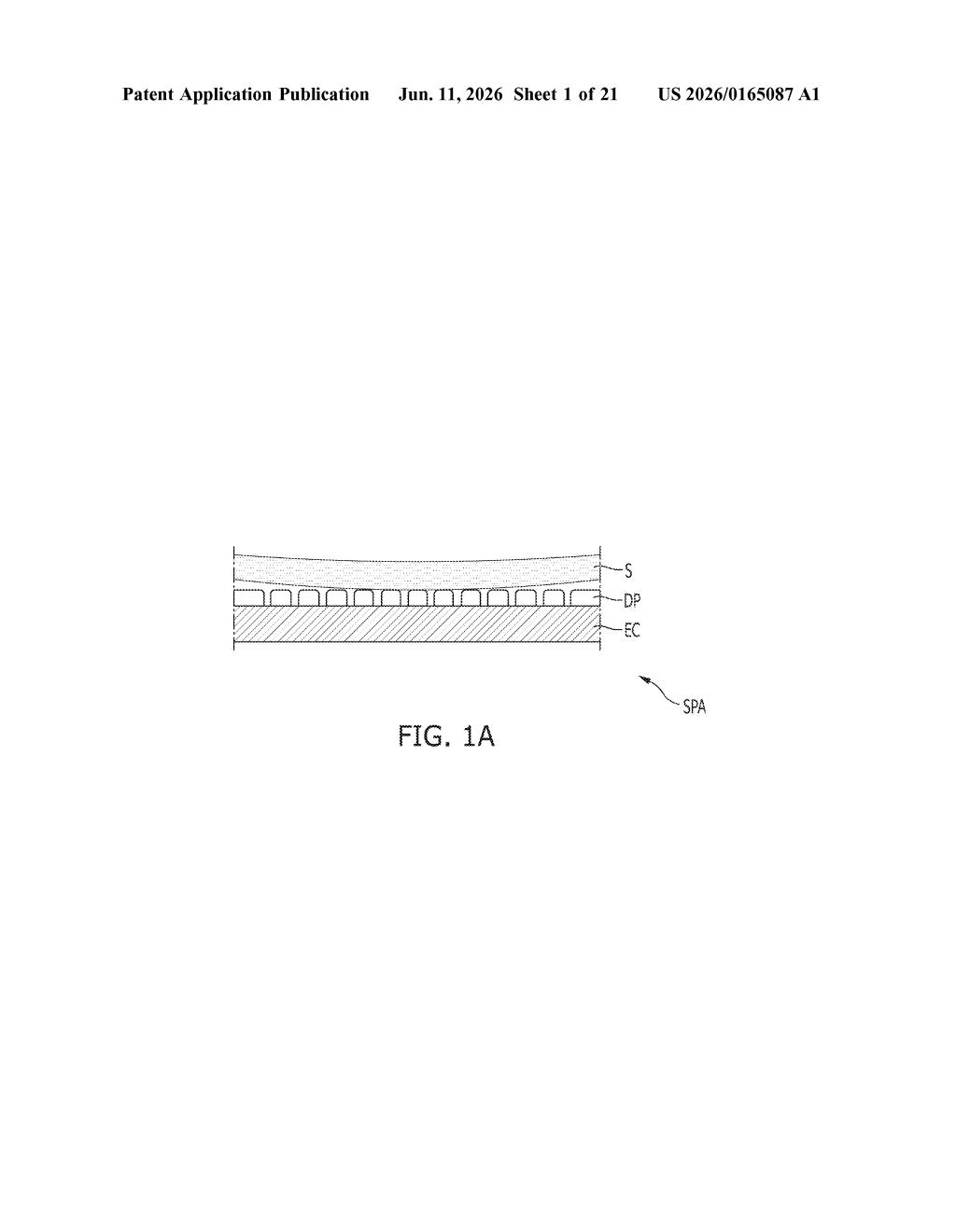
The patent covers a substrate processing apparatus — the kind of vacuum chamber used in semiconductor fabrication for steps like etching or deposition (adding or removing thin layers of material on a wafer).
The chamber has four key components working together:
- Electrostatic chuck (ESC): A platform in the lower part of the chamber that holds the wafer in place using electrostatic force — essentially clamping it without mechanical clamps — and includes a built-in heater to bring the wafer to the right temperature for processing.
- Showerhead: A perforated plate at the top of the chamber that distributes processing gas evenly across the wafer surface, like a sprinkler spreading water uniformly.
- Planarization member: The novel addition — a component that actively applies downward pressure to at least one region of the wafer, pushing it flat against the chuck during processing.
The combination of heat (from the ESC heater) and mechanical pressure (from the planarization member) is designed to correct wafer bow — a common problem where wafers curve slightly, especially as they get thinner or after earlier processing steps have introduced stress into the material.
What wafer flatness means for cutting-edge chip yields
Wafer flatness is one of the semiconductor industry's less-glamorous obsessions, but it's critically important as chip geometries shrink. Even a few micrometers of bow can push a wafer outside the focus range of the lithography tools used to print circuit patterns, causing defects across an entire batch. Yield — the percentage of usable chips per wafer — drops, and costs rise.
For Samsung, which competes fiercely with TSMC and SK Hynix in both logic chips and memory, squeezing out yield improvements at the equipment level is a real competitive lever. If this approach reduces wafer-bow-related defects during processing, it could translate directly to more good chips per wafer — which matters enormously at the volumes Samsung operates.
This is squarely a manufacturing-process patent, not a consumer-product story. It won't show up in a phone spec sheet, but it's exactly the kind of incremental tooling improvement that quietly determines who can produce the most chips at the lowest defect rate. Worth noting for anyone tracking Samsung's semiconductor equipment strategy.
Get one Big Tech patent every Sunday
Plain English, intelligent commentary, no hype. Free.
Editorial commentary on a publicly published patent application. Not legal advice.