Samsung Patents a Touch Electrode Layout That Places Gaps Near Connection Points
Samsung Display is rethinking where to put the empty spaces inside touchscreen electrodes — and the exact placement turns out to matter more than you'd expect.
What Samsung's touch electrode gap design actually does
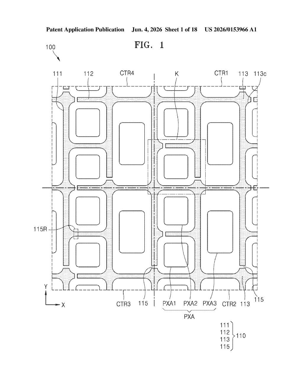
Imagine drawing a cross (+) on a piece of conductive film — that cross is basically what a touch electrode looks like inside your phone screen. It has arms extending in two directions, joined at a center point. The question engineers wrestle with is: where do you cut tiny gaps into that shape, and why?
Samsung's patent describes a touch electrode design where small gaps (called separation areas) are deliberately placed close to the junction where the two arms meet, rather than out near the tips of each arm. That precise positioning is the core of what they're filing here.
The idea is that by controlling exactly where the electrode material is absent, Samsung can tune how electrical signals travel across the touchscreen grid — potentially reducing interference between neighboring electrodes or improving how reliably the screen reads your finger's position.
How the separation area interacts with the electrode geometry
The patent describes a touch electrode shaped like a cross or plus sign, with a first extension area running horizontally and a second extension area running vertically. The point where they meet is called the connection area.
The key innovation is a separation area — a void or gap that contains none of the electrode's conductive material. What's specific here is its placement rule: this gap must sit closer to the connection area (the junction) than to the midpoint of either arm. In other words, the gap lives near the center of the cross, not near the tips.
- First extension area: the electrode arm running in one direction (e.g., horizontal)
- Second extension area: the arm running in the crossing direction (e.g., vertical)
- Connection area: the junction where both arms meet
- Separation area: a material-free zone positioned near that junction
By specifying the longitudinal position of the gap relative to the arm's length, Samsung is effectively patenting a geometric rule for electrode design — one that could affect parasitic capacitance (unwanted electrical coupling between adjacent electrodes) and the sensitivity of touch detection across the panel.
What this means for Samsung's display touch performance
Touch electrode geometry is one of those deeply unsexy engineering problems that directly affects how accurately your finger is tracked on a display, especially as screens get thinner and pixel densities climb. If Samsung can reduce crosstalk between electrodes through smarter gap placement, that translates to sharper touch precision on future Galaxy phones, tablets, or foldables — without necessarily adding new hardware layers.
This is also relevant as Samsung Display supplies panels to other device makers. Any improvement baked into the electrode layout propagates across a wide range of products. That said, this is an incremental geometry refinement, not a wholesale rethink of how touch panels work.
This is a narrow, component-level patent covering a specific geometric rule for touch electrode design — the kind of filing that rarely makes headlines but quietly shapes the precision of every touchscreen Samsung ships. It's worth noting if you follow display supply chain engineering, but it's not a signal of any major product direction.
Get one Big Tech patent every Sunday
Plain English, intelligent commentary, no hype. Free.
Editorial commentary on a publicly published patent application. Not legal advice.