Samsung Patents a New Wiring Layout for Chips Stacked Inside a Single Package
When chip designers stack multiple memory dies on top of each other inside a single package, the wiring that connects them can get messy fast — especially when power lines and data lines compete for the same space. Samsung's latest patent describes a specific layout meant to bring order to that tangle.
What Samsung's stacked-chip wiring patent actually does
Imagine a tiny skyscraper where each floor is a separate computer chip. The chips need to talk to each other and to the outside world, all through incredibly thin wires — some carrying data, some carrying power. Fitting all of those wires without them interfering with each other is one of the harder problems in chip packaging.
Samsung's patent describes a three-chip stack where each chip has a carefully assigned role for which wires connect where. The key trick: the power and ground connection on the top chip is positioned close to the middle chip's pad rather than near its own center. That placement shortens the power wire, which can reduce electrical noise and voltage swings that hurt performance.
This is plumbing-level work — you won't see it advertised on a spec sheet. But getting these connections right is what separates a chip package that runs reliably at high speed from one that doesn't.
How the power and signal wires are routed across three chip layers
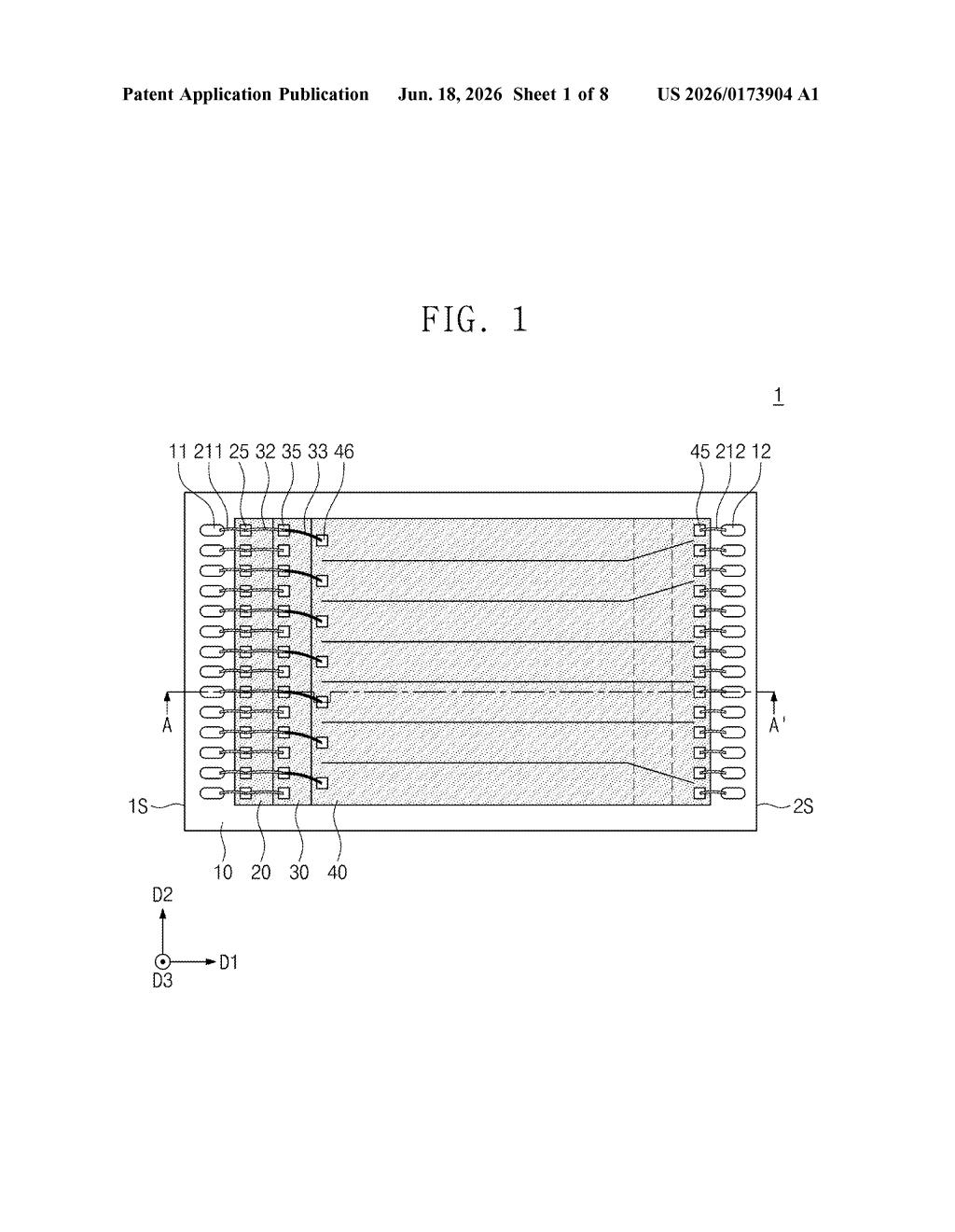
The patent covers a semiconductor package — a self-contained module that houses three chips (called dies) stacked vertically on a shared substrate, like floors on a building's foundation.
Each chip communicates through thin bond wires — actual metal wires, not the embedded copper traces used in more expensive through-silicon-via packages. The substrate at the bottom has two sets of channel pads (connection points for data signals), one for the lower portion of the stack and one for the upper portion. This separates the data paths so different chips don't share the same wire route.
The defining design choice is where the power-ground pad sits on the third (top) chip. Rather than placing it near the top chip's own data pad, the layout positions it closer to the second chip's pad below it. This shortens the wire that carries power and ground, which matters because:
- Shorter power wires have lower resistance and inductance
- Lower inductance means less voltage bounce when current demand changes quickly
- Steadier voltage translates to more reliable chip operation at speed
The first connection wire bridges the first and second chips for data, while a separate power-ground wire runs up to the third chip — keeping signal and power paths distinct.
What this means for dense memory chip packaging
Stacked-die packaging is how the industry fits more memory into less physical space — it's the architecture behind high-bandwidth memory (HBM) modules used in AI accelerators and the DRAM stacks inside mobile chips. As stacks get taller and data rates climb, the placement of every wire becomes a meaningful engineering decision rather than a detail.
Samsung's approach here is incremental rather than transformational, but incremental wins in packaging are exactly what separate competitive memory products from also-rans. If this layout reduces noise on the power rail, it could allow higher clock speeds or lower failure rates without changing the underlying chip design — a cost-free gain that matters in high-volume production.
This is a quiet, unglamorous patent about bond-wire placement inside a chip stack. It won't headline a product launch. But Samsung's memory packaging group files patents like this precisely because small wiring optimizations compound into real yield and performance advantages at scale — and that's where memory market share is actually won.
Get one Big Tech patent every Sunday
Plain English, intelligent commentary, no hype. Free.
Editorial commentary on a publicly published patent application. Not legal advice.