
Sony
Sony · Chip · Filed May 6, 2025 · USPTO published Jun 18, 2026 · Jun 18 release
Sony Patents a Way to Slow Light Down and Make Sensors Far More Precise
Sony is patenting a way to make light travel more slowly through a tiny ring-shaped optical circuit — and that trick, if it works as described, could make sensors like LiDAR dramatically more precise.
- Publication number
- US 2026/0169224 A1(US20260169224A1)
- Applicant
- SONY SEMICONDUCTOR SOLUTIONS CORPORATION
- Filed · Published
- May 6, 2025 · Jun 18, 2026
- Inventors
- Haruhiko TERADA
- Status when we published
- Waiting for an examiner
- Document
- 21 claims
- US classification
- 356/5.1
- Parent application
- National Stage Entry of PCT/JP2023/037361 (filed Oct 16, 2023)(PCTJP2023037361)
What Sony's light-slowing ring resonator actually does
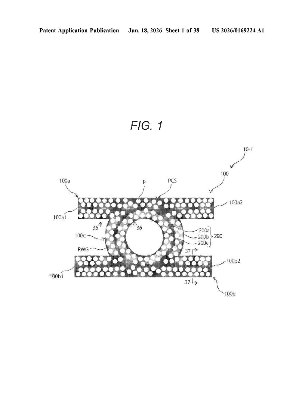
Picture a racetrack for light. Normally, light zips around so fast that any measurement you take has very little time to react to subtle changes. Sony's patent describes a special racetrack — a ring-shaped optical waveguide — with a photonic crystal structure built into it. That structure is essentially a repeating microscopic pattern etched into the material that forces light to slow down significantly as it travels.
When light slows down inside the ring, the device becomes far more sensitive to tiny changes in the environment around it — things like how far away an object is, or how a signal is shifting. Think of it like the difference between trying to read a street sign from a speeding car versus a slow bicycle.
This kind of technology sits at the core of optical sensors and light-based communication chips. Sony Semiconductor, the division behind image sensors in most of your smartphones, is clearly investing in the next layer of sensing hardware.
How a photonic crystal structure increases the group refractive index
The patent covers a ring resonator — a circular loop of material that guides light around and around, letting it build up intensity and interact with itself. Ring resonators are standard building blocks in photonic chips, used in everything from optical modulators (which encode data onto light) to distance-measuring sensors.
The key addition here is a photonic crystal structure (PCS) integrated directly into the waveguide wall. A photonic crystal is a material with a periodic (repeating) internal pattern at nanometer scale — similar in concept to how a crystal's atomic lattice interacts with X-rays, but tuned to interact with visible or near-infrared light. This pattern creates what engineers call a slow-light effect, increasing the group refractive index (essentially a measure of how slowly the light pulse travels through the material).
Slowing the light has a compounding benefit: it increases the effective optical path length without making the physical ring any bigger, which sharpens the resonator's sensitivity to phase shifts. The patent title also lists several intended applications:
- Optical modulators (encoding signals onto light beams)
- Light source devices
- Distance measuring devices (LiDAR-style sensors)
- General resonator devices
The claim itself is intentionally broad — it covers any ring resonator whose waveguide incorporates a photonic crystal structure.
What this means for Sony's LiDAR and distance-sensing hardware
Sony Semiconductor Solutions is the world's largest image sensor maker, and it has been expanding into LiDAR and 3D sensing for automotive and robotics markets. A more sensitive ring resonator could translate directly into sharper distance measurements, which matters a lot when a self-driving car is trying to distinguish a pedestrian from a trash can at 40 mph.
That said, this is a foundational component patent — the kind that sits several engineering layers below anything you would ever directly touch. Its real value is as a building block that other Sony chips could incorporate. Whether that happens depends on whether the slow-light gain survives the manufacturing tolerances of real-world chip fabrication, which is where many elegant photonics ideas stall out.
Source: US 2026/0169224 A1 at the USPTO (PDF). Full patent text and figures are in the official publication.
Get our take in your Top Stories
Liked this breakdown? Add Patentlyze as a preferred source on Google, and our plain-English take shows up more often in your Top Stories the next time Sony patent news breaks.
Add Patentlyze on Google
One click.
There are more where this came from
We read every patent application Big Tech publishes and send you the ones worth knowing. Plain English, free, every week.
More from Sony
All 707 Sony patents →


More in Chip
All 645 Chip patents →
AMD
Xilinx Patents a Chip That Throttles Itself Based on the Math It's Doing

Qualcomm
Qualcomm Patents a Video Chip That Cuts Its Own Power During Low-Quality Streams
Intel
Intel Patents a Chip Trick That Runs AI Math in Tinier 4-Bit Numbers

AMD