
Samsung Patents Stacked Memory Chips That Each Tune Their Own Signal Strength
When you stack several memory chips on top of each other, the ones at the bottom and the ones at the top are not in identical electrical situations, and that difference can silently corrupt data. Samsung's new patent addresses exactly that problem.
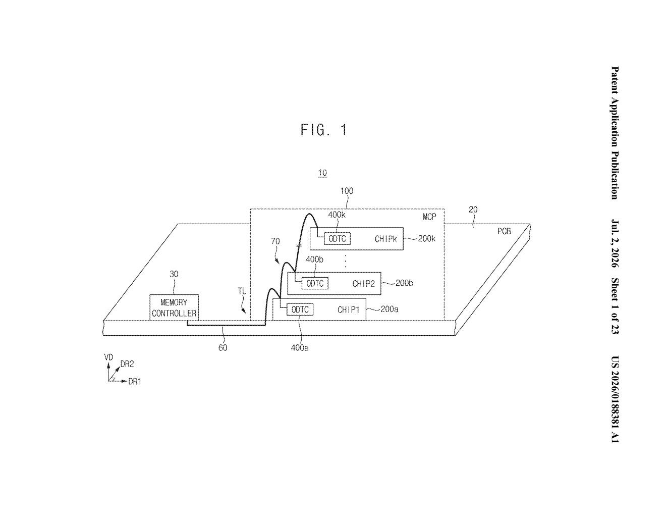
What Samsung's position-aware memory stack actually does
Imagine a block of apartments connected by the same shared hallway. The apartment on the ground floor and the one on the top floor are both connected, but getting a signal to travel cleanly to each one is a different challenge depending on how far away you are from the entrance.
That's roughly what happens inside a stacked memory package, the kind found in phones, laptops, and servers. Multiple memory chips are layered on top of each other and share a single wire for communication. Each chip sits at a different distance from the circuit board below, so the electrical signal arriving at each one has slightly different characteristics.
Samsung's patent lets each chip in the stack automatically adjust its own electrical resistance based on its position in the stack. Instead of every chip using the same fixed setting, each one knows where it sits and tunes itself accordingly, keeping signals clean across the whole stack.
How each chip reads its position and sets its own resistance
The patent covers a multi-chip package (MCP), a design where multiple memory chips are physically stacked on a single circuit board and share one signal wire to talk to the rest of the system.
The core problem is signal integrity. When a signal travels down a shared wire and hits multiple chips, reflections and interference build up. Engineers use a technique called on-die termination (ODT), essentially a resistor built directly onto each chip, to absorb those reflections. The catch: the right resistance value depends on where a chip sits in the stack, because the electrical path length differs for each position.
Traditionally, all chips in a stack might use the same ODT setting, which is a compromise that satisfies no chip perfectly. Samsung's invention gives each chip its own ODT circuit and lets it set its resistance independently based on position information, meaning which layer it occupies relative to the circuit board surface.
- Each memory chip stores or receives information about its physical position in the stack.
- That position data feeds into the chip's ODT circuit, which selects the appropriate resistance value.
- The result is that every chip in the stack is individually tuned, reducing signal noise across all layers simultaneously.
What this means for high-speed memory reliability
As memory chips get stacked higher and data rates get faster, the margin for signal error shrinks. A chip tuned for the wrong position in a stack can slow down communication or require retransmissions, costing both speed and power. This patent points toward denser, faster memory packages that don't have to trade off reliability to achieve their stacking density.
For Samsung, which supplies memory to most of the world's smartphone and server makers, this kind of incremental reliability improvement compounds across billions of devices. You probably won't see this feature advertised on a spec sheet, but it's the kind of engineering that lets future chips push higher speeds without becoming unstable.
This is careful, unglamorous engineering work on a real and well-documented problem in stacked memory design. It won't spark headlines about a new product, but it's the type of foundational patent that actually ships inside hardware. Worth a look if you follow semiconductor packaging trends.
Get our take in your Top Stories
Liked this breakdown? Add Patentlyze as a preferred source on Google, and our plain-English take shows up more often in your Top Stories the next time Samsung patent news breaks.
There are more where this came from
We read every patent application Big Tech publishes and send you the ones worth knowing. Plain English, free, every week.
Want this weekly breakdown for a company we don't cover? Patentlyze Pro →