
Samsung's New Patent Makes Every Corner of a Touchscreen Respond at the Same Speed
The farther a touch signal has to travel inside your screen, the more likely it is to arrive late or distorted. Samsung's latest patent describes a wiring layout designed to keep every part of a touchscreen responding at exactly the same speed.
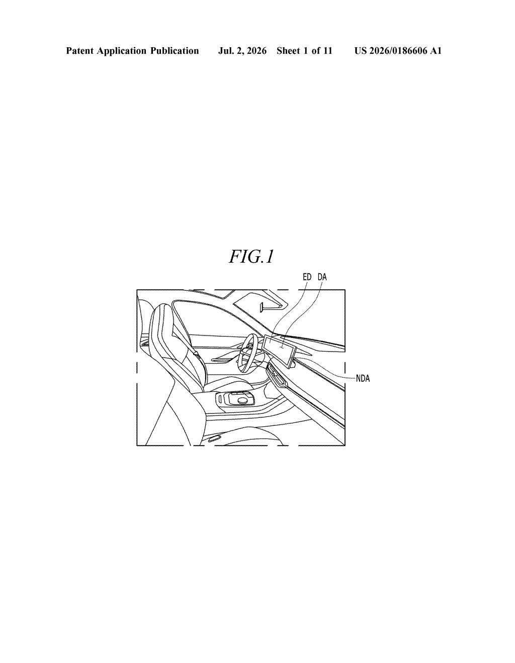
What Samsung's touch-signal balancing trick actually does
Imagine a touchscreen as a grid of tiny sensors, each one waiting to detect your finger. The sensors near the edge of the screen are farther from the chip that reads them, so their signals take longer to arrive. That tiny difference in travel time can cause some parts of the screen to feel slightly less responsive than others.
Samsung's patent tackles this with a clever wiring workaround. Sensors that are physically close to the reader chip get connected through longer wires inside the circuit board, while sensors that are farther away get shorter wires. The total path length ends up roughly equal for every sensor, so the chip receives all the signals at the same time.
The design uses a multi-layer circuit board, meaning some wires run on one level of the board while others run on a different level, letting Samsung pack more wire length into a small space without the wires crossing and interfering with each other.
How Samsung equalizes wire lengths across the circuit board
The patent describes a display module built around a "self-dot" touch detection method, where each sensor fires and reads itself individually rather than working in a coordinated grid. This puts extra pressure on timing consistency because every sensor is acting independently.
The key components are:
- Sensors spread across the display area, each paired with a multiplexor (a switching chip that routes the signal onward)
- Spider lines, the traces that carry signals from the multiplexors along the non-display border of the screen to the edge connectors. Sensors closer to the edge have shorter spider lines; sensors farther away have longer ones.
- Flexible printed circuit boards (FPCs) that bridge the display panel to a main circuit board
- Connection lines on the circuit board that deliberately compensate for spider-line length differences. A short spider line is paired with a long connection line, and vice versa, so the combined path is equalized.
Critically, the patent specifies that portions of a single connection line can be routed through different layers of the circuit board. That layer-jumping is what allows a longer wire to fit physically in the same board footprint as a shorter one, making the whole compensation scheme practical in a real device.
What this means for large-screen and foldable displays
Touch latency differences across a screen are usually invisible to users in normal use, but they become more noticeable on larger panels, such as tablets, monitors, and foldable phones, where the physical distance from edge sensors to the reader chip grows significantly. A consistent signal path means the display's firmware can use simpler, faster processing without needing software patches to correct for timing offsets.
For Samsung specifically, this kind of wiring precision matters as its display division supplies panels to a wide range of devices beyond its own phones. A manufacturable, hardware-level fix for signal timing is the kind of foundational work that can improve touch feel across an entire product lineup without any changes to software.
This is unglamorous but genuinely useful engineering. Equalizing signal path lengths in hardware is cleaner than patching timing in firmware, and the multi-layer routing approach is a real solution to a real constraint. It won't make headlines at a product launch, but it's the kind of detail that separates a display that feels crisp from one that feels slightly off.
Get our take in your Top Stories
Liked this breakdown? Add Patentlyze as a preferred source on Google, and our plain-English take shows up more often in your Top Stories the next time Samsung patent news breaks.
There are more where this came from
We read every patent application Big Tech publishes and send you the ones worth knowing. Plain English, free, every week.
Want this weekly breakdown for a company we don't cover? Patentlyze Pro →