Samsung Patents Selective Metal Deposition Process for Memory Cell Transistors
Building a transistor inside a memory chip is a bit like trying to paint the inside of a thimble — precision is everything. Samsung's latest patent describes a way to deposit metal exactly where it needs to go, and nowhere else.
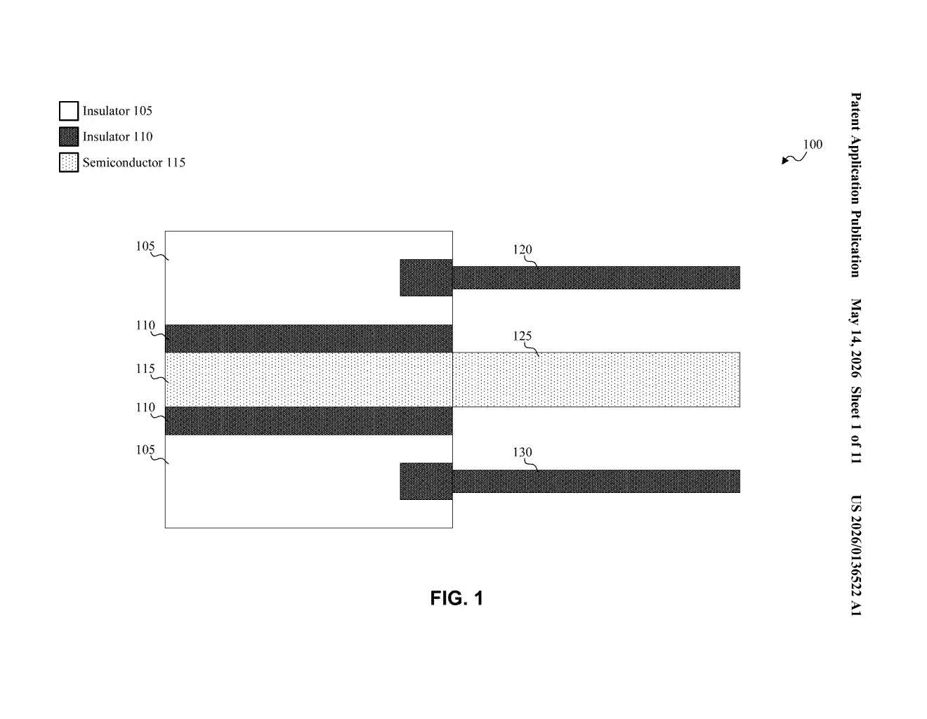
What Samsung's layered metal recess trick actually does
Imagine trying to fill only one specific crack in a wall with putty, without getting any on the surrounding surface. That's roughly what chipmakers face when building the tiny transistors inside memory cells — they need metal in very specific spots, and stray deposits cause problems.
Samsung's patent describes a multi-step process where engineers carve out a small recess in an insulating layer, coat surfaces with a dielectric (a kind of electrical barrier), lay down an initial metal layer, strip away the parts they don't want, and then selectively grow a second metal layer only inside that carved-out recess.
The result is a transistor gate structure where the metal sits precisely where it should, potentially reducing electrical leakage and improving how tightly transistors can be packed together. For you as a consumer, that could eventually translate into faster, denser memory chips inside your phone or laptop.
How Samsung layers metals inside a precision recess
The patent describes a fabrication sequence for a memory cell transistor — the kind found in DRAM or flash storage — using a technique called selective metal deposition (depositing metal only on chosen surfaces, not everywhere).
The process steps are:
- Form the structural trio: a first insulator, a second insulator, and a semiconductor channel (the active region through which current flows).
- Etch a recess by removing part of the first insulator — creating a controlled cavity where the gate metal will ultimately sit.
- Apply a dielectric layer (an electrically insulating film that separates the gate metal from the channel, acting as the gate oxide) across the relevant surfaces.
- Deposit a first metal layer over the dielectric, then selectively remove portions of it — a patterning and etch step that clears metal from areas outside the recess.
- Grow a second metal layer selectively on top of the remaining first metal layer, exclusively inside the recess.
The two-metal approach likely serves a dual purpose: the first metal sets up the work function (which controls the transistor's switching threshold), while the second metal fills the recess to form a low-resistance gate electrode. This is consistent with buried-wordline DRAM architectures, where transistor gates sit recessed below the silicon surface to reduce short-channel effects.
What this means for next-gen DRAM and flash scaling
Memory scaling has been hitting physical limits for years — the closer you pack transistors, the more they interfere with each other. Buried-gate DRAM architectures help by sinking the gate into the substrate, but that only works if you can deposit metal precisely into a deep, narrow recess without contaminating adjacent structures. Samsung's selective two-layer approach is a direct answer to that problem.
For the memory industry, finer control over gate metal placement means potential gains in data retention, leakage current, and ultimately chip density. Samsung competes hard with SK Hynix and Micron on DRAM node advancement, and process patents like this are part of the toolkit that determines who ships the densest chips first.
This is a process engineering patent — not flashy, but exactly the kind of incremental fabrication innovation that decides whether Samsung's next DRAM node ships on time or slips. The selective two-metal deposition scheme for buried-gate transistors is a real technical problem, and this patent shows Samsung has at least one documented solution in hand.
Get one Big Tech patent every Sunday
Plain English, intelligent commentary, no hype. Free.
Editorial commentary on a publicly published patent application. Not legal advice.