
Samsung Patents a Processor That Lets Different Memory Types Work Together Seamlessly
Modern chips often have to talk to two or more completely different kinds of memory at once, and right now that conversation is clunky and slow. Samsung's new patent describes a processing core designed to sit in the middle and translate fluently between them.
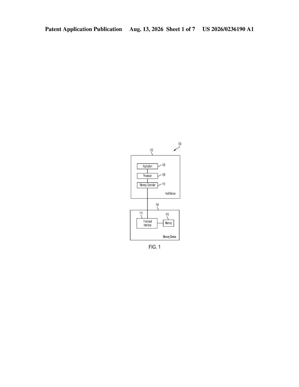
What Samsung's memory-translation core actually does
Every time your phone or laptop runs an app, several different kinds of memory are working at the same time, passing instructions back and forth. When those memory types speak different "languages," the chip has to stop and work out the translation, which burns time and energy.
Samsung's patent describes a dedicated processing core built specifically to handle that translation job. When it receives an instruction written for one type of memory, it figures out the right way to rewrite that instruction for a different type of memory and sends it along. While the slower memory is doing its job, the core uses its own small, fast internal buffer to keep things moving without waiting around.
The result is that a chip can work with multiple memory types without the usual speed penalty. Think of it like a real-time interpreter at a meeting: instead of the whole room grinding to a halt while one person explains what another said, the interpreter keeps the conversation flowing.
… generating, by the processing circuit, a second command for a memory controller associated with a second memory type different from the first memory type; …
Translation: The chip translates commands so one type of memory can talk to a completely different type.
How the processing circuit converts and buffers commands
The patent describes a memory-communications core, a dedicated processing circuit that acts as a translator between different memory types inside a chip system.
Here is how the core handles a single operation:
- It receives a command written for one type of memory (say, a fast, on-chip cache format).
- It determines the correct processing protocol for that command, essentially the rulebook for how to convert it.
- It generates a new, equivalent command formatted for a second, different memory type (such as main DRAM), and sends that translated command to the appropriate memory controller.
- Simultaneously, it performs whatever local bookkeeping is needed on its own internal buffer, a small, very fast scratchpad that is quicker to access than the external memory being targeted.
The key idea is that the core does not sit idle while the slower memory processes the translated command. By offloading local tasks to the on-chip buffer and dispatching translated commands in parallel, the circuit avoids the back-and-forth stalling that normally happens when two memory systems have to coordinate.
The patent covers both the method (the sequence of steps) and the system (the hardware circuit that carries them out), which means Samsung is staking out territory over both the process and the physical implementation.
… wherein the buffer has a lower latency for performing the task than the second memory type.
Translation: It uses a fast internal cache to handle tasks much quicker than standard memory can.
What this means for chips juggling multiple memory types
As chips pack in more types of memory, including different cache layers, high-bandwidth memory, and traditional DRAM, the overhead of coordinating between them eats into performance. A dedicated translation core could make that overhead much smaller, which matters for everything from AI accelerators to server processors where memory bandwidth is often the main bottleneck.
For Samsung, which makes both memory chips and the processors that use them, this kind of patent sits at a natural intersection of its product lines. The company publishes a steady stream of filings in the chip architecture space, and plain-English patent summaries of that work show a consistent push toward tighter integration between processing and memory, a direction the whole semiconductor industry is moving in.
The patent describes new hardware, a dedicated processing circuit, which means this is further from shipping than a pure software change would be: Samsung would need to design, tape out, and validate a chip that physically includes this core before any product sees it. That said, the concept maps directly onto real engineering problems Samsung already deals with in its memory and processor divisions, so the shortest path to a product is probably an internal system-on-chip where Samsung controls both sides. The document is specific enough about the buffer and protocol-translation mechanism to read like engineering work already underway.
There are more where this came from
We read every patent application Big Tech publishes and send you the ones worth knowing. Plain English, free, every week.
The drawings
7 drawing sheets from US 2026/0236190 A1 · click any drawing to enlarge


Want this weekly breakdown for a company we don't cover? Patentlyze Pro →
Be the first to weigh in