
Sony Patents a Light-Based Sensor That Reads Data Through Walls and Skin
Sony has filed a patent for a miniature laser that fires in the infrared range, the same light used in fiber-optic communications, while consuming far less energy than conventional designs, thanks to an unusual crystal structure that traps light rather than letting it leak away.
What Sony's perovskite infrared laser actually does
Every time a fiber-optic cable carries your video call across a city, a tiny laser at one end converts electricity into invisible infrared light. Those lasers need to be efficient: the more energy they waste as heat or stray light, the worse the signal gets.
Sony's new patent describes a laser built around a material called perovskite, a crystal that has gotten a lot of attention in solar-cell research because it handles light in unusual ways. The key twist here is a microscopic surface pattern, smaller than a wavelength of light, that creates a condition physicists call a BIC mode (short for "bound state in the continuum"). In plain terms, the pattern keeps light circling inside the laser instead of escaping prematurely, which means the laser can start firing with far less input power.
The result, at least on paper, is an infrared laser that could be smaller, cheaper to run, and easier to integrate into optical chips than existing designs.
A laser device comprising: a laser light generating unit having a nanostructure configured to exhibit a BIC mode and including a perovskite material, the laser light generating unit being configured to oscillate infrared light.
Translation: The device uses a special crystal structure and a specific mineral material to create an invisible infrared laser beam.
How the nanostructure traps light to lower the firing threshold
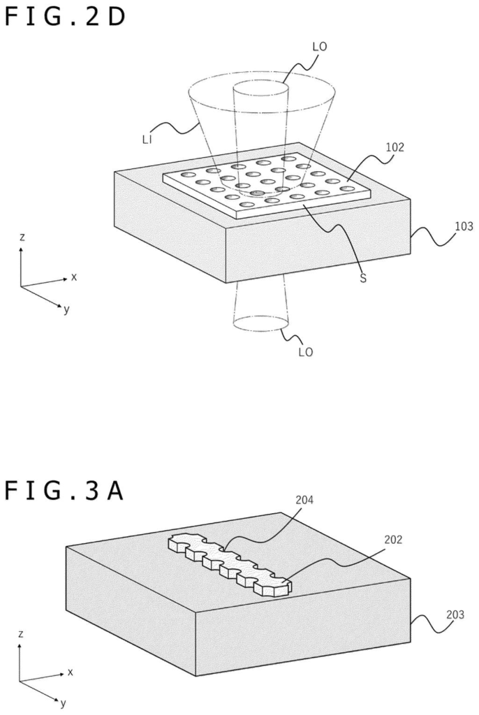
The patent covers a laser device built around two interacting technologies: a perovskite material and a nanostructure, a surface or layer patterned at nanometer scale (roughly a thousand times thinner than a human hair).
- Perovskite is a family of crystalline materials originally studied for solar cells. Sony's filing applies it to lasers because perovskite can absorb and emit light efficiently across a useful range of wavelengths, including the infrared bands used in fiber-optic communications.
- BIC mode stands for "bound state in the continuum." Normally, light leaks out of a laser cavity unless the design confines it tightly. A BIC structure exploits interference effects so that light that would ordinarily escape instead stays trapped, dramatically lowering the oscillation threshold, the minimum energy needed to get the laser lasing.
- Zero refractive index is an optional feature mentioned in the patent. A material with zero refractive index bends light in an extreme way, making the phase of the light wave constant throughout the material. This can make the laser output more coherent and uniform.
The nanostructure can be formed either directly from the perovskite material itself or from a conventional dielectric (non-conducting) material embedded inside the perovskite layer, giving engineers design flexibility. The target output is infrared light in the communication wavelength band, roughly 1300-1550 nanometers.
The nanostructure may be configured to exhibit a zero refractive index. For example, the nanostructure may be formed by the perovskite material, or the nanostructure may be formed by a dielectric material, and provided in the perovskite material.
Translation: The sensor can be designed to have a zero refractive index, which allows light to pass through it without bending.
What this means for future sensors and optical chips
Infrared lasers are load-bearing infrastructure for modern communications. Every long-distance internet cable, every data-center interconnect, and an increasing number of on-chip optical links depend on compact, efficient infrared sources. The dominant technology today is indium phosphide, which works well but is expensive to manufacture and hard to integrate directly onto standard silicon chips. A perovskite-based laser that genuinely achieves a lower firing threshold could make optical interconnects cheaper and more power-efficient at scale.
For Sony specifically, this intersects with its sensing and imaging businesses. LIDAR sensors, time-of-flight cameras, and industrial scanners all use pulsed infrared lasers, and a lower-threshold design translates directly into longer battery life or smaller form factors. The patent is one data point in a broader wave of photonics filings that plain-English patent summaries from Sony and its peers have been tracking as the industry pushes optical technology closer to the chip level.
This is the third battery and power filing from Sony we've tracked since June, joining one on solar cells in controllers and one on robot walking power.
Every optical connection inside a data center leaks energy as heat, and the lasers that drive those connections are a primary culprit. At the scale of millions of links running around the clock, even a small reduction in how much power each laser needs to fire up translates into meaningful savings on electricity and cooling.
Sony's approach bets on a class of materials that can produce light more efficiently by exploiting a physics phenomenon that traps energy inside a tiny structure instead of letting it scatter away. The science behind that is credible, and the efficiency gains it promises match the size of the problem.
The durability of those materials under real operating heat and humidity is the open question this patent does not answer, and that gap between a promising lab result and a component that ships in actual hardware is where many strong ideas stop moving forward.
Get our take in your Top Stories
Liked this breakdown? Add Patentlyze as a preferred source on Google, and our plain-English take shows up more often in your Top Stories the next time Sony patent news breaks.
There are more where this came from
We read every patent application Big Tech publishes and send you the ones worth knowing. Plain English, free, every week.
The drawings
9 drawing sheets from US 2026/0254190 A1 · click any drawing to enlarge


Want this weekly breakdown for a company we don't cover? Patentlyze Pro →
Be the first to weigh in