
IBM Patents a Precise New Switch to Link Quantum Computing Components More Reliably
Getting two quantum bits to talk to each other without accidentally disturbing everything around them is one of the hardest engineering problems in quantum computing. IBM has filed a patent for a coupler design that tries to solve it by chaining three ultra-sensitive circuit elements in a single tunable switch.
What IBM's double transmon coupler does for quantum chips
Ever tried adjusting the volume on one speaker without changing the sound on every other speaker in the room? That is roughly the problem IBM is wrestling with in quantum computers, where turning up the interaction between two quantum bits (qubits) can inadvertently disturb neighboring bits.
This patent describes a small circuit called a double transmon coupler that sits between two qubits and acts like a precision dial. You can tune it to let the qubits communicate with each other when needed, then dial the interaction back to nearly zero when you want them to stay separate. The trick is a chain of three tiny, temperature-sensitive junctions inside the coupler that gives it a wider and more flexible tuning range than a single-junction design.
The result, in theory, is a quantum chip where each pair of qubits can be switched on and off more cleanly, which matters enormously as IBM and others try to scale quantum processors up from dozens of qubits to thousands.
… a flux-tunable inductive coupler which comprises a superconducting loop that couples the first transmon and the second transmon, the superconducting loop comprising a third Josephson junction …
Translation: A magnetic loop connects the two main circuit parts using an extra superconducting valve.
How three Josephson junctions control qubit coupling strength
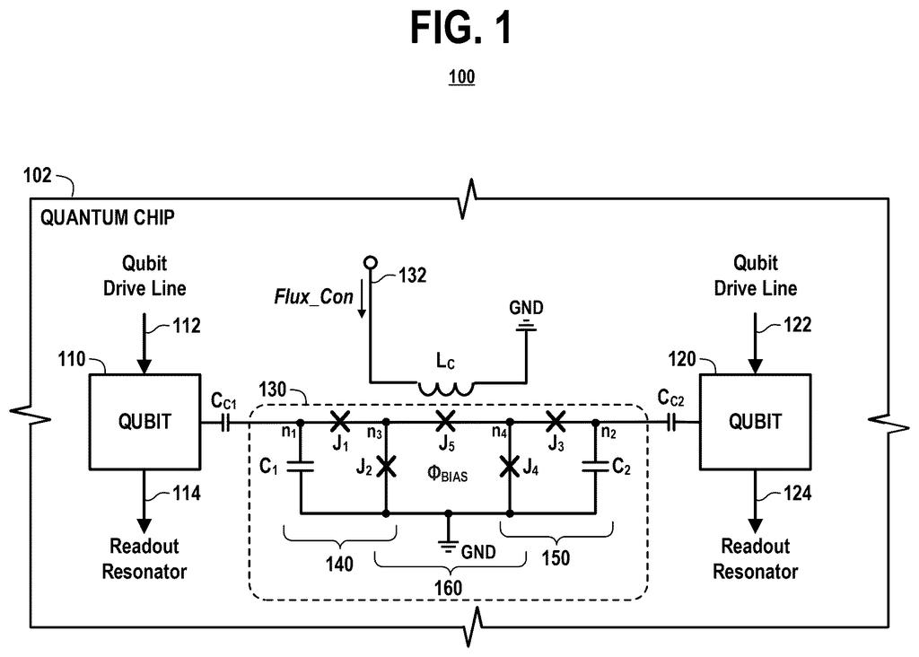
The coupler is built from two transmons (a type of superconducting qubit used as a tunable circuit element rather than as a data-carrying qubit itself) linked by a flux-tunable inductive coupler, which is a small superconducting loop whose properties change when you thread a magnetic field through it.
The key architectural choice is that three Josephson junctions (nanoscale barriers between two superconductors through which quantum current can tunnel) are wired in series between the coupler's two connection points. One junction lives inside each transmon; the third lives inside the superconducting loop that connects them.
Wiring them in series rather than in parallel changes the effective energy landscape of the coupler. This gives engineers a broader tunable range: by threading different amounts of magnetic flux through the loop, they can sweep the coupler's behavior across a wider spectrum, turning the qubit-to-qubit interaction strongly on, completely off, or to precise intermediate values.
- First node: connects the coupler to qubit one
- Second node: connects the coupler to qubit two
- Flux-tunable loop: the magnetic-field-sensitive element that sets coupling strength
The architecture is fully superconducting, meaning it operates at temperatures near absolute zero, consistent with existing IBM quantum hardware.
The first Josephson junction, the second Josephson junction, and the third Josephson junction are coupled in series between the first node and the second node of the tunable coupler.
Translation: Three microscopic switches are wired together in a chain to control the link between the qubits.
What this means for building larger, more reliable quantum processors
For quantum computers to solve problems beyond today's toy demonstrations, they need many qubits working together with low error rates. A major source of errors is residual coupling: qubits that are supposed to be ignoring each other still nudge each other slightly, corrupting calculations. A coupler with a wider tuning range and a cleaner off-state directly attacks that problem.
IBM has been filing steadily around superconducting qubit control for years, and this fits a clear pattern of iterative hardware refinement rather than a single dramatic leap. If this design performs in the lab the way the math suggests, it could become a building block in future generations of IBM's Heron or successor quantum processors, improving gate fidelity without requiring a wholesale redesign of the chip architecture.
That makes this IBM's 20th filing we've tracked since May in our quantum computing buildout watch, following one on auto-selecting error settings and one on modular error-free programs.
Measured against what it takes to ship a working product, this patent describes a circuit diagram, not a finished component. Before anything reaches a real quantum computer, IBM's engineers need to physically build test versions, measure whether the design actually suppresses unwanted interference between qubits across the brutal cold and precise magnetic conditions these chips require, and confirm the approach survives the inevitable imperfections of mass fabrication.
That gap is normal and expected. Foundational hardware ideas like this typically precede product improvements by two to five years in quantum computing.
The meaningful question is whether the wider control range this design promises translates to fewer errors in real multi-qubit operations, and that answer will live in an experimental paper that does not yet exist.
There are more where this came from
We read every patent application Big Tech publishes and send you the ones worth knowing. Plain English, free, every week.
The drawings
8 drawing sheets from US 2026/0268193 A1 · click any drawing to enlarge


Want this weekly breakdown for a company we don't cover? Patentlyze Pro →