
Samsung Patents a Method to Keep Storage Chips From Clashing During Data Transfers
When a storage chip finishes sending data, the next chip in line has to know exactly when to start talking, or the two streams collide. Samsung's new patent describes a method for a memory controller to precisely time that handoff, embedding delay instructions directly inside the signal that wakes up the next chip.
What Samsung's staggered flash memory timing actually does
Imagine your phone needs to pull up a large file that's spread across multiple memory chips inside its storage. Each chip has to take a turn sending its slice of that data back to the controller. If one chip starts talking before the previous one has finished, the signals crash into each other and everything has to be retried.
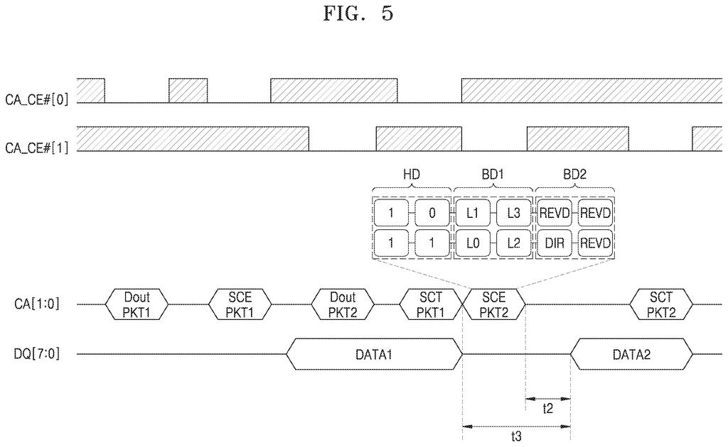
Samsung's patent describes a smarter handoff process. Before the first chip has even finished sending its data, the controller pre-loads a special timing instruction into the command it sends to the second chip. That instruction tells the second chip exactly how long to wait before it starts outputting data, so the two chip outputs never overlap on the shared wire.
The practical goal is a cleaner, faster read cycle across multi-chip storage. You wouldn't see a settings toggle for this; the benefit would show up as slightly faster load times or fewer silent read errors in devices that use high-density NAND flash, like smartphones, SSDs, and memory cards.
transmit a first data output command address packet to a first non-volatile memory die among the plurality of non-volatile memory dies, through a command address bus, receive a first data from the first non-volatile memory die through a data bus …
Translation: The controller asks the first memory chip for data and waits to receive it over the shared bus.
How the controller delays the second chip's data output
Modern flash storage packages several individual memory dies (independent chips stacked or arranged together) behind a single controller. When the controller needs data that spans multiple dies, it has to read from them in sequence, because they all share one data bus (the physical wire carrying data back to the controller).
The patent describes how the controller structures the command sequence:
- It sends a read command to the first die and begins receiving that data.
- Before that transfer ends, it sends a read command packet to the second die, followed immediately by a "select chip enable" packet that activates the second die.
- Embedded inside that select chip enable packet is a second body field containing "first delay information", essentially a countdown telling the second die how many clock cycles to wait before it starts placing data on the shared bus.
- Finally, it sends a "select chip terminate" command to the first die, formally ending its turn.
The key innovation is packing the timing delay instruction inside the chip-select packet itself, rather than using a separate timing signal or forcing the controller to calculate and apply the delay after the fact. This keeps the two dies' output windows from overlapping on the shared data bus, preventing a condition called bus contention (where two chips try to drive the same wire at once, corrupting both signals).
… sequentially outputs a second data output command packet that instructs a second non-volatile memory die among the plurality of non-volatile memory dies to output second data, a second select chip enable packet that selects the second non-volatile memory die, and a first select chip terminate command packet that terminates selection of the first non-volatile memory die.
Translation: It carefully juggles commands to shut down the old chip and wake up the new one in order.
What this means for storage speed in real devices
For most people, storage errors are invisible until they aren't. A phone that reboots unexpectedly, a file that won't open, or a laptop SSD that slows to a crawl under load can all trace back to low-level timing problems inside the flash package. A tighter handoff mechanism like this one reduces the margin for error at the hardware level, which matters most as flash packages keep stacking more dies into the same small space.
Samsung keeps filing on flash memory timing and die coordination, which reflects how competitive the high-density NAND market has become. Faster, denser storage is only useful if the controller can reliably orchestrate all those chips. For you as a buyer, improvements here tend to show up as more consistent read performance rather than a single peak-speed number on a spec sheet.
Samsung's 34th filing we've tracked since June in our next-gen SSD applications watchlist builds on earlier work including one about drives running out of instructions and one about drives reporting their own data status.
For someone using a laptop or phone, this patent works entirely in the background, solving a problem you would never name but might occasionally feel: a brief stutter when opening a large file, or a read error that makes you reopen an app. The fix coordinates how multiple memory chips take turns sharing a single data line, so they hand off cleanly instead of colliding.
You would only notice this working if it stopped working. That makes it more valuable in professional storage equipment and high-endurance drives than in everyday consumer devices, where the stakes of a mistimed handoff are lower.
The improvement is a small one, tucking timing instructions inside a packet that the system was already sending rather than adding a separate step. Small refinements like this are how storage hardware gets more reliable over years of iteration, and reliability is the one thing users most take for granted until it disappears.
There are more where this came from
We read every patent application Big Tech publishes and send you the ones worth knowing. Plain English, free, every week.
The drawings
20 drawing sheets from US 2026/0277490 A1 · click any drawing to enlarge


Want this weekly breakdown for a company we don't cover? Patentlyze Pro →