
Samsung Patents Technology That Catches Data Errors Inside Storage Chips Automatically
Your phone's storage chip has to trust that its own internal wiring is working perfectly, and right now there's no easy way to double-check that without outside help. Samsung's new patent describes a system where the chip's controller and memory can run a verification test entirely on their own.
How Samsung's storage chip checks its own accuracy
Ever noticed your phone slow to a crawl when saving a file, or wondered why SSDs sometimes corrupt data silently? A lot of that comes down to whether the tiny controller chip and the memory cells it manages are actually communicating cleanly.
Samsung's patent describes a built-in self-test where the controller generates a test pattern from a starting number called a seed, then tells the memory chip to independently generate the same pattern and compare results. If both patterns match, the communication path is working. If they don't, something has gone wrong and the device can flag it before your files are at risk.
The clever part is that neither side has to send the test data back and forth over the wire, each generates it locally from the same seed. That keeps the test fast and self-contained, running on the device without needing your computer or phone to do the heavy lifting.
… the memory controller includes a training module configured to generate first pattern data based on a seed, and wherein the control logic circuit includes a pattern data check circuit configured to: generate second pattern data based on a first training command and the seed; and compare the first pattern data and the second pattern data.
Translation: The storage device creates a secret code to verify that data is being read and written correctly without errors.
How the seed-based pattern comparison actually runs
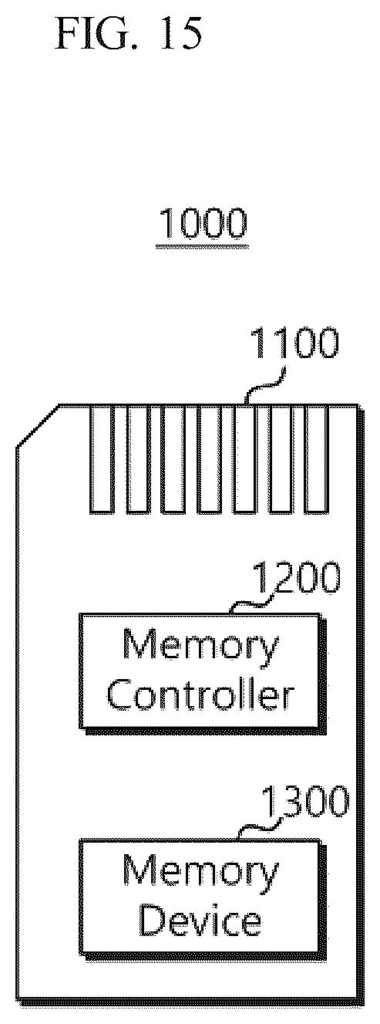
The patent describes a storage device made up of two main parts: a memory controller and a memory device (think of the controller as the manager and the memory cells as the filing cabinets).
The controller has a training module that generates a block of test data called first pattern data, derived from a shared starting value called a seed. At the same time, the controller sends a first training command and the seed over to the memory chip's own logic circuit.
Inside the memory chip, a dedicated pattern data check circuit takes that seed and independently generates its own matching block of test data, the second pattern data. It then compares the two:
- If they match, the signal path and timing between controller and memory are confirmed good.
- If they don't match, there is a detectable error in the interface or the internal logic.
A page buffer circuit temporarily holds any data sensed from the actual memory cells during normal operation, and can play a role in the verification flow. The key insight is that generating patterns locally on each side, rather than shipping raw test data across the interface, makes the test faster and avoids the very channel it is trying to verify as a bottleneck.
A storage device includes a memory device that includes memory cells, and a memory controller that controls the memory device. The memory device includes a memory cell array that includes the memory cells, a control logic circuit that writes or senses data in or from the memory cell array in response to a command received from the memory controller …
Translation: This technology uses a central controller to manage how data is stored and retrieved from the memory chips.
What this means for flash storage reliability
Flash storage reliability is one of those things users only notice when it fails. Silent data corruption or intermittent errors inside an SSD or smartphone storage chip are notoriously hard to diagnose because the problem lives between two silicon components that rarely report issues proactively. A self-contained verification loop like this one could let devices catch interface drift, manufacturing defects, or wear-related signal degradation before they turn into lost files or system crashes.
For Samsung, which supplies storage chips to a huge range of consumer electronics makers as well as its own Galaxy devices, baking a test like this into the chip's own control logic is the kind of reliability feature that enterprise buyers and phone OEMs care about at scale. Memory controller self-testing sits alongside a broader wave of chip-level diagnostics appearing across Big Tech patent news, as storage makers push more intelligence down into the hardware itself.
Samsung's 30th filing we've tracked since June in our next-generation SSD work builds on earlier applications like one cutting save wait times and one on drive overheating.
The shortest route to a product here is actually short. Samsung is not proposing new materials, new cell geometries, or a new manufacturing process, the patent describes logic circuits and a comparison routine that could be implemented in firmware and silicon that already exist in principle. The main question is whether the seed-based pattern check is accurate enough to catch the failure modes that matter most in real devices, which is an engineering validation problem, not a fundamental research problem. That makes this filing feel less like a distant research bet and more like a description of something that could slot into a next controller revision with modest effort.
There are more where this came from
We read every patent application Big Tech publishes and send you the ones worth knowing. Plain English, free, every week.
The drawings
15 drawing sheets from US 2026/0245646 A1 · click any drawing to enlarge


Want this weekly breakdown for a company we don't cover? Patentlyze Pro →
Be the first to weigh in