Samsung Patents Storage Hardware That Quietly Reroutes Data Around Its Own Defects
Even brand-new memory chips can have microscopic manufacturing flaws. Samsung's latest patent describes a flash memory design that quietly sidesteps those flaws on its own — across two stacked layers of storage cells at once.
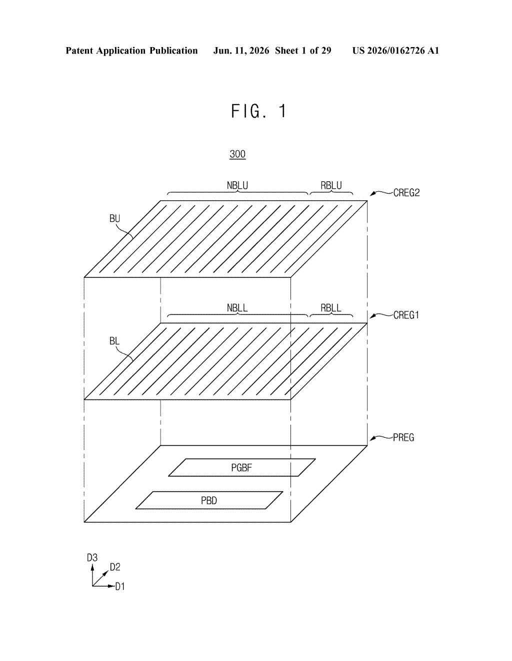
How Samsung's stacked memory patches its own bad lines
Imagine a city grid where a few streets are permanently blocked. Rather than tearing up the whole grid, traffic engineers reroute cars around the blocked roads using pre-built detour lanes. Samsung's patent works on the same idea, but inside a flash memory chip.
Flash memory chips — the kind that store data in your phone or SSD — are manufactured at such a tiny scale that some data pathways, called bitlines, inevitably come out flawed. Normally that means a portion of the chip is wasted. Samsung's design includes dedicated spare bitlines built into each layer of the chip, ready to substitute for any bad ones that turn up.
What's new here is that the chip handles two stacked layers of memory cells together. A single central circuit identifies all the defective lines across both layers and reassigns traffic to the spare lanes — all without you ever noticing a problem.
How the page buffer decoder consolidates faulty bitlines
The patent describes a 3D nonvolatile memory chip (the category that includes the NAND flash in most modern SSDs and smartphones) built with two cell regions stacked vertically on top of each other.
- First cell region — the lower layer of storage cells, containing both normal bitlines and spare (redundant) bitlines.
- Second cell region — the upper layer, also equipped with its own normal and spare bitlines.
- Peripheral circuit region — sits below both layers and contains the page buffer circuit (the temporary workspace that holds data while it's being read or written) and the key new component: the page buffer decoder.
The page buffer decoder is the brain of the repair operation. It surveys defective bitlines from both cell layers simultaneously, consolidates that defect map into one unified picture, and then reroutes reads and writes through the redundant bitlines. This cross-layer coordination is the core claim — earlier approaches typically managed defect repair one layer at a time, which wastes spare capacity.
By pooling spare lines across both layers, the decoder can make more efficient use of the built-in redundancy, potentially allowing the chip to survive a higher number of manufacturing defects before being discarded.
What self-repairing flash means for chip yield and reliability
For Samsung, this is fundamentally a manufacturing yield story. Every chip that survives quality checks instead of being thrown out is money saved — and as NAND flash stacks grow taller (some chips now exceed 200 layers), the chance that a given bitline comes out faulty only increases. A repair mechanism that works across layers rather than within a single layer helps keep that yield high without requiring more physical spare lines, which eat into storage density.
For you as a consumer, the downstream effect is flash storage that's more reliable and potentially cheaper to produce — which eventually shows up in SSDs, smartphones, and USB drives. It won't make headlines the way a new processor does, but quiet improvements in how chips handle their own imperfections are a big reason storage has gotten so affordable.
This is a routine but genuinely useful memory-engineering patent — the kind of incremental yield-improvement work that keeps Samsung's flash business competitive without making any consumer-facing splash. It's not a product announcement, and it's not a research breakthrough; it's a well-defined solution to a real manufacturing problem that gets more pressing as chips stack higher.
Get one Big Tech patent every Sunday
Plain English, intelligent commentary, no hype. Free.
Editorial commentary on a publicly published patent application. Not legal advice.