
Nvidia Files Patent for a Two-Camera Inspector That Spots Flaws on Circuit Boards
A flaw on a circuit board can hide from one camera and show up clearly under another. Nvidia's patent application describes software that looks through two cameras at once and merges what they see to catch it.
What Nvidia's two-camera inspector actually does
Every time a circuit board rolls off a factory line, somebody has to make sure it isn't flawed. A single board can carry more than eight hundred parts, some as small as 0.1 millimeter, so a bad solder joint is easy to miss with the naked eye, or even with one camera.
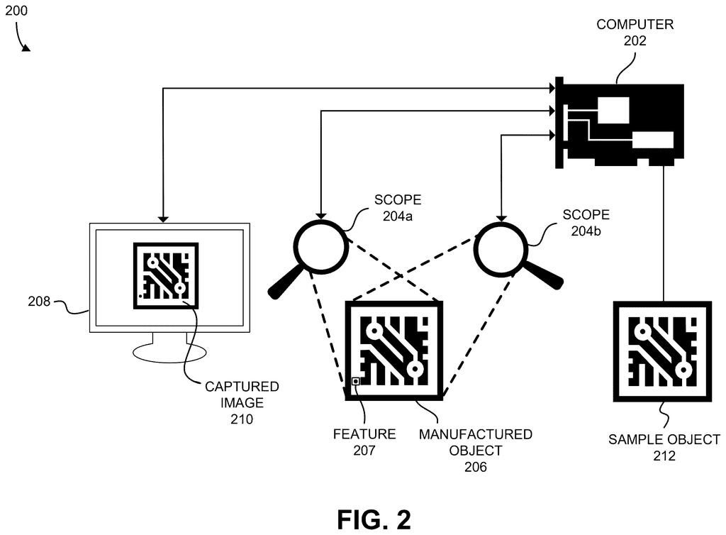
Nvidia's patent application describes a setup with two cameras that look at the same board in different ways, such as from different angles or under different lighting. A neural network (software loosely modeled on the brain and trained on examples) pulls the important details out of each view and blends them into one combined picture. That blend makes the flaw stand out from everything around it.
The system then compares the result with a flawless reference board. If something doesn't match, it flags the defect, and it can even tell the assembly line to kick the board out for a human to look at.
… combine the first and second image data into a composite representation of the object that accentuates a feature of the object by causing the one or more processors to: determine, by providing the first and second image data as input to a set of convolutional layers of a neural network, a set of feature maps …
Translation: The system blends images from two cameras using a neural network to highlight specific details.
How the two views get blended into one picture
The application covers processors that take pictures of one object from two cameras at different viewpoints and then decide whether the object has a defect. The key step is how the two pictures get merged.
- Convolutional layers (filters that scan an image for edges, lines and colors) turn each picture into feature maps, which mark what stands out.
- Fully connected layers turn those maps into feature vectors (lists of numbers describing what the network saw).
- Concatenation (joining those lists end to end) produces one composite representation. The claim says this increases the contrast between the flaw and the background.
The two cameras can capture different kinds of light, such as visible light plus infrared, ultraviolet or X-ray, and one of them can sit inside a microscope. The filing's main example uses a pair of identical networks (a Siamese network) that compare the board against a golden sample, a defect-free reference. A defect is flagged when the distance between the two grows too large.
The output can include a box drawn around the flaw, its location, and a trigger to pull the object off the line. The description says it can run on a small single-board computer such as an Nvidia Jetson Nano, handling six to eight video streams at once.
… generating a set of feature vectors by providing the set of feature maps from the set of convolutional layers to a set of fully connected layers of the neural network, and concatenating the set of feature vectors to increase contrast between the feature and one or more background features.
Translation: Data layers are combined to make the flaws stand out more against the background.
Why cheaper inspection matters on the factory floor
If you own a phone, car or laptop, you depend on circuit boards that someone had to check. This filing is aimed at cheaper, portable inspection that can switch between camera angles and lighting setups, which its background says older inspection machines handle poorly. A rig built from a small computer and USB microscopes, as the description lays out, points toward inspection that doesn't need a dedicated, costly machine.
The description also lists other jobs: sorting paper, plastic and metal at a recycling plant, or checking toppings on frozen pizzas. For Nvidia, it shows another use for the small AI computers it already sells, since its own Jetson board is the example hardware. Remember this is a patent application, not a product.
Nvidia's 44th filing we've tracked in Enterprise AI since May adds to a run that includes one on robot indoor location and one on loading partial AI models.
Missing a bad solder joint is an expensive mistake. One faulty board can become a dead gadget or a recalled batch, and the parts are small enough that a single camera angle can hide the problem. The filing's own background complains that older inspection machines are costly, slow and built for one task.
Giving the software two views and a clean reference board fits a problem of this size. A flaw that glints under one light and vanishes under another gets two chances to show itself. The portable hardware also matters, because a small factory could actually afford to try it.
The recipe uses well-known image analysis building blocks arranged for a factory job, so don't expect a surprise. Its value depends on how few good boards it wrongly rejects, and the filing gives no accuracy numbers to judge that.
Get our take in your Top Stories
Liked this breakdown? Add Patentlyze as a preferred source on Google, and our plain-English take shows up more often in your Top Stories the next time Nvidia patent news breaks.
There are more where this came from
We read every patent application Big Tech publishes and send you the ones worth knowing. Plain English, free, every week.
The drawings
56 drawing sheets from US 2026/0320775 A1 · click any drawing to enlarge


Show the other 48 sheets


Want this weekly breakdown for a company we don't cover? Patentlyze Pro →
Be the first to weigh in