
Sony Files Patent for Tiny Structures That Even Out the Picture in Wearable Displays
The most interesting detail is how local this gets: Sony describes giving each region of an AR lens its own microscopic pattern, tuned to make the image brighter and more even.
What Sony's patterned AR lens actually does
Ever pointed a flashlight at a wall and noticed the bright blob in the middle fading toward the edges? Spreading light evenly is harder than it sounds, and it is a real challenge for glasses that float an image in front of your eye.
In AR glasses, light from a tiny projector travels inside the lens, bouncing between its surfaces, until it reaches a patch of microscopic ridges and bumps that sends it out toward your pupil. Sony's filing describes dividing that patch into regions and giving each region its own pattern of tiny shapes. The rotation, size or outline of those shapes changes from one region to the next.
The idea is that each part of the lens can be tuned separately, so the picture comes out brighter and more uniform across your view. The filing also describes stacking two layers of shapes on top of each other for even more control.
An output coupling grating (OCG) for a waveguide-based display, comprising: a base substrate; and a plurality of unit cells arranged in groups on the base substrate …
Translation: The patent describes a special grating built on a base layer to help project images in wearable displays.
How the tiny tiles change across the lens
The filing covers one specific part of an AR display: the output coupling grating (OCG), the patch of the lens that lets image light out toward your eye. Light from a small projector enters the lens through an input grating, then travels along inside by total internal reflection (bouncing off the inner surfaces instead of escaping) until it reaches the OCG.
The OCG is a base layer covered in repeating unit cells, tiny parallelogram-shaped tiles spaced a few hundred nanometers apart (the filing gives 200 to 620 nm; a nanometer is a billionth of a meter). Each tile holds a small raised or sunken shape called a photonic structure. Cells are grouped into regions, and every cell in a region has the same shape, size and rotation. Different regions get different ones.
The filing describes several ways to vary those shapes:
- Rotated shapes: a parallelogram turned inside its tile, sometimes with different angles than the tile.
- Cropped shapes: a parallelogram with corners trimmed away, exposing the layer below, with the trimmed and untrimmed ends lined up along the direction the light travels.
- Stacked layers: a second shape on top of the first, with a different outline.
- Many-sided shapes: one claim covers shapes with an even number of sides above six, each side parallel to at least two others.
The shapes can be bumps or dents, are described as 1 to 500 nm tall, and can be made with nanoimprint lithography (stamping nanoscale patterns) or inkjet printing.
One or more of the first orientation, the first size, and the first shape of the first photonic structure are different than the second orientation, the second size, and the second shape of the second photonic structure.
Translation: Tiny light-bending structures are varied in shape, size, and direction across the display to make the picture look even.
Why even brightness matters for AR glasses
Glasses that float images in front of your view depend on how the picture looks: how bright it is, and whether it stays even from one part of your view to another. Sony's filing says its pattern design is meant to improve both brightness and uniformity, and it does that at the surface of the lens itself.
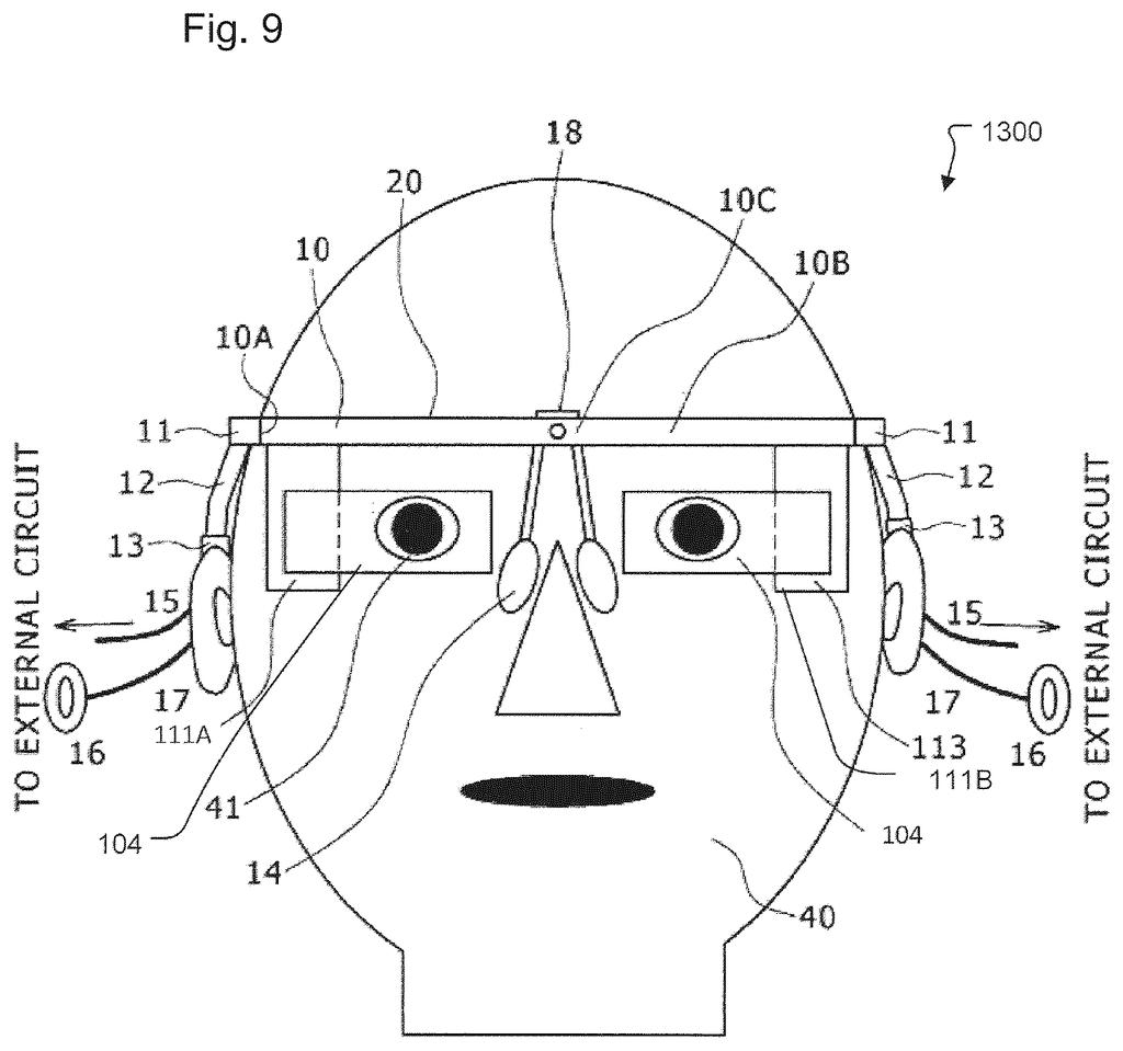
The filing describes a head-mounted display with a waveguide (the light-carrying lens) in front of each eye, so the target is wearable AR or mixed reality glasses. Nothing in the text names a product, and it gives design rules and size ranges rather than measured results, so treat it as one ingredient a lens maker could use.
Sony's 42nd filing we've tracked since July in the AR glasses race builds on slimmer gaze-tracking glasses and blink-timed glitch hiding.
This one sits at the component level. It needs no new device and no new software: the change is a pattern on the lens surface, made with stamping or printing methods the filing names. That makes it a plausible swap-in for a team already building a waveguide display.
What has to exist first is the rest of the glasses: a projector, a lens that carries the light, and a layout for where each region sits. The text offers shape rules and size ranges but no measured gains in brightness, so the size of the improvement stays unknown.
The shortest route to a product is a lens maker adopting these patterns in its next waveguide. For you, that would show up as a nicer picture in whichever glasses use it, which makes this a useful but routine optics refinement.
Get our take in your Top Stories
Liked this breakdown? Add Patentlyze as a preferred source on Google, and our plain-English take shows up more often in your Top Stories the next time Sony patent news breaks.
There are more where this came from
We read every patent application Big Tech publishes and send you the ones worth knowing. Plain English, free, every week.
The drawings
9 drawing sheets from US 2026/0329087 A1 · click any drawing to enlarge


Show the other 1 sheets

Want this weekly breakdown for a company we don't cover? Patentlyze Pro →
Be the first to weigh in