
Samsung Patents a Flattening Fix for the Tiny Layered Films Inside Wearable Displays
Building a lens out of structures smaller than a wavelength of light sounds impressive until the whole thing warps. Samsung's new patent is about a surprisingly fiddly problem: how do you keep a nanoscale optical film flat when different parts of it are built differently?
What Samsung's nano-lens flattening trick actually does
Ever tried to stack two different materials and ended up with a surface that buckles in the middle? That's roughly the problem Samsung is trying to solve here, except at a scale far too small to see.
Modern AR lenses (the kind that might sit inside a pair of smart glasses) use layers of microscopic patterns to bend and focus light. The catch is that the patterned zone and the unpatterned border around it have different thicknesses. That mismatch creates tiny hills and valleys across the lens surface, which causes focusing errors and makes it harder to stack more layers on top cleanly.
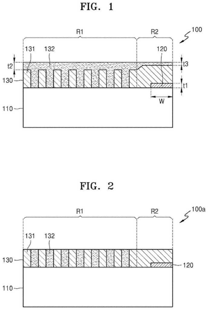
Samsung's idea is to place a small reflective pad under the flat border region to physically prop it up, so the whole stack sits at the same height. There's a twist: the pad is deliberately smaller than the border area it supports, and it's pulled slightly away from the edge of the patterned zone. That gap prevents any stray light from leaking into the image area while still doing the leveling job.
… a reflective pad disposed between the lower optical layer and the nanostructure layer to face the non-active region of the nanostructure layer …
Translation: A tiny mirror layer sits underneath to support the edges of the film.
How the reflective pad offsets and the dual-dielectric fill work
The patent describes a three-layer sandwich. At the bottom is a lower optical layer (a base that also handles light). On top of that sits the nanostructure layer, which is divided into two zones: an active region where tiny pillars of one dielectric material (think: a transparent insulator that bends light) are etched into precise patterns, and a non-active region around the edges where no etching happens.
Because only the active region is patterned, a height difference opens up between the two zones. Samsung fills the gaps between the pillars with a second dielectric material that has a different refractive index (meaning it bends light by a different amount). That fill planarizes the surface somewhat, but the border still needs extra support.
The reflective pad lives in the gap between the lower layer and the nanostructure layer, directly under the non-active border. Two design details in claim 1 are specific:
- The pad's edge is set back from the boundary between the active and non-active zones by a deliberate offset distance.
- The pad's footprint is smaller than the non-active region it sits under.
The setback and the smaller size together ensure the pad never intrudes into the image-forming area, so the reflective material doesn't scatter or redirect light that should be passing cleanly through the lens.
… a first dielectric patterned in the active region and unpatterned in the non-active region and a second dielectric filled between patterns of the first dielectric …
Translation: The optical layer alternates between patterned and solid sections made of different materials.
What this means for thinner, cleaner AR optics
AR glasses live or die by optical quality. Even a slight warp in a lens stack can produce ghost images, reduced contrast, or a display that only looks sharp in the center. If Samsung can reliably planarize these nanostructure films during manufacturing, it becomes easier to build lenses that are both thin and optically clean, which is the combination that's kept most AR products bulky or blurry for years.
For consumers, the downstream effect would be lighter, better-looking glasses that don't require thick frames to hide chunky optics. For the industry, a manufacturable planarization approach matters because nanostructure lenses are only useful at scale if you can stack them consistently. Samsung's interest in AR optics manufacturing shows up across its recent work in display and lens IP, and this filing fits that pattern.
Samsung's 57th filing we've tracked since May in the AR glasses race builds on one clearing graphics for focus and one for pushing 3D icons, adding another piece to how the company is shaping its AR display and input ideas.
Claim 1 protects a very specific geometry: a reflective pad sandwiched between two layers, deliberately undersized and pulled back from the edge of the active optical zone. Samsung owns that particular offset arrangement, not reflective pads or multilayer lenses in general.
That narrowness has real consequences. Anyone who sizes or positions the pad differently avoids the claim entirely, but if this exact set-back configuration turns out to be the only manufacturable path to flat, reliable AR lenses, that narrow slice becomes the only slice that matters.
Whether this holds up depends on whether the patent contains hard data showing why that specific gap produces better results. Experimental evidence makes the claim defensible; description alone probably does not.
There are more where this came from
We read every patent application Big Tech publishes and send you the ones worth knowing. Plain English, free, every week.
The drawings
23 drawing sheets from US 2026/0299179 A1 · click any drawing to enlarge


Want this weekly breakdown for a company we don't cover? Patentlyze Pro →
Be the first to weigh in