IBM Patents a Co-Packaged Optical Module for High-Density Chip Interconnects
As AI clusters demand ever-faster chip-to-chip links, IBM is patenting a way to embed optical hardware directly inside a chip package — shrinking the distance light has to travel and cutting the energy wasted in the process.
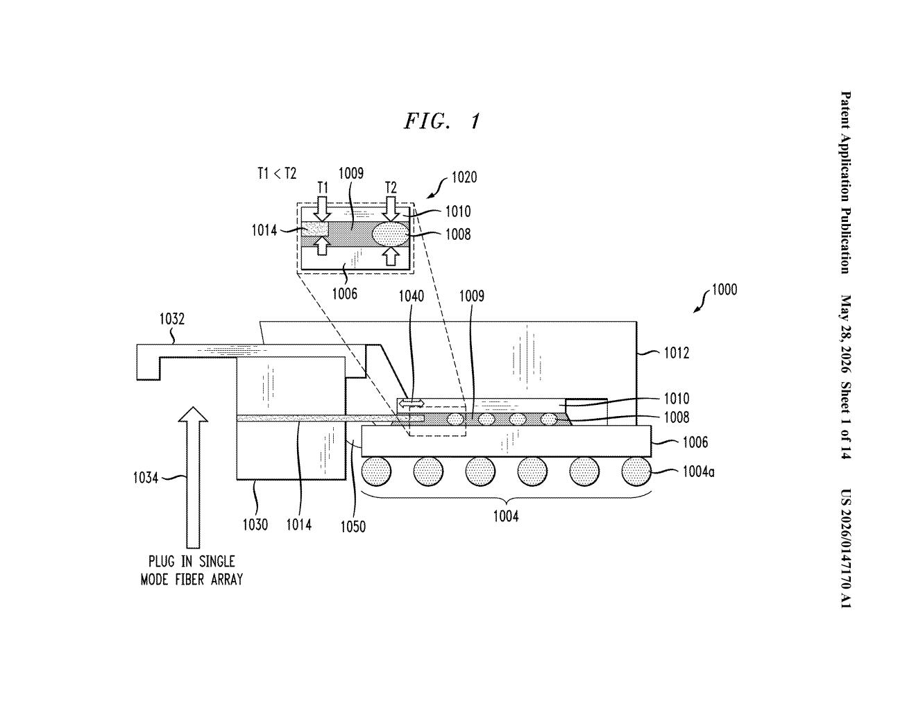
What IBM's co-packaged optical module actually does
Imagine your computer's processor and its networking hardware are miles apart, connected by a long copper wire. Every time data crosses that wire, a little energy is lost and a little time is wasted. Now imagine moving the networking hardware into the same tiny package as the processor itself. That's the core idea behind co-packaged optics.
Instead of sending electrical signals across a circuit board to reach a separate networking chip, IBM's design tucks a photonic integrated circuit — a chip that sends and receives data using light instead of electricity — directly into the same module as your main processor. A protective lid clamps directly onto the substrate (the base the chip sits on), sandwiching everything together tightly.
The result is a compact package that can survive the high-heat solder reflow process used in manufacturing, while keeping optical signal losses low and data throughput high. It's the kind of behind-the-scenes plumbing work that makes the next generation of AI hardware actually go faster.
How IBM sandwiches the photonic chip inside the lid assembly
The patent describes an optical module built around four key components working together:
- Photonic integrated circuit (PIC) — a chip that transmits data as pulses of light rather than electrical signals, enabling much higher bandwidth over short distances with lower power consumption.
- Substrate — the base layer the PIC is mounted on, analogous to a PCB but purpose-built for this assembly.
- Lid — a structural cover that makes direct contact with the substrate (not the PIC itself), so the PIC is enclosed in the cavity between them. IBM specifies this lid can sit either above or below the PIC depending on the configuration, giving packaging engineers flexibility.
- Optical waveguides and ferrule — waveguides are tiny channels (like fiber-optic wires at chip scale) that carry light to and from the PIC; the ferrule is the connector that couples those waveguides to an external fiber link.
The design's key engineering constraint is solder reflow compatibility — meaning the whole assembly can go through the high-temperature ovens used in standard electronics manufacturing without the optical alignment drifting or the materials delaminating. That's a notoriously hard problem in photonics packaging, and IBM's direct lid-to-substrate contact approach is one strategy for managing the mechanical stress.
What this means for AI datacenter bandwidth bottlenecks
Datacenter interconnects are one of the biggest bottlenecks holding back large AI training runs. Copper links between chips burn energy and cap bandwidth; moving to optical connections solves both problems, but only if the photonics hardware can be integrated cheaply and reliably at scale. Co-packaged optics — putting the photonic chip right next to the compute chip in the same package — is the industry's leading bet for closing that gap.
For you as a reader, this doesn't show up as a product feature anytime soon. But for hyperscalers buying IBM server hardware or custom AI accelerators, a manufacturing-compatible co-packaged optical module is the kind of component that could meaningfully cut the cost and power draw of the next wave of AI infrastructure.
This is deep-stack infrastructure work — not flashy, but exactly the kind of patent that matters if IBM wants a seat at the table in AI datacenter buildouts. The specific focus on solder reflow compatibility and insertion loss tells you this isn't a blue-sky concept; it reads like a real engineering solution to a real manufacturing problem IBM has been wrestling with. Worth watching as co-packaged optics move from research demos to production silicon.
Get one Big Tech patent every Sunday
Plain English, intelligent commentary, no hype. Free.
Editorial commentary on a publicly published patent application. Not legal advice.