Samsung Patents a Shared-Memory System for Running Multiple AI Chips Together
Running multiple AI chips in parallel sounds great until they all need the same data and nobody's coordinating the handoff. Samsung's new patent is specifically about solving that traffic-jam problem.
What Samsung's multi-NPU memory routing actually does
Imagine your phone is running a complex AI task — say, real-time video enhancement — and it needs to spread that work across several dedicated AI chips at once. Each chip needs to read and write data, but if they're all working from separate memory buckets, you waste time and power copying the same information around.
Samsung's patent describes a management layer that sits above all those AI chips and asks two questions before any data gets stored: Is this data going to be used by more than one chip? And is there a shared pool of memory available right now? If both answers are yes, the data goes into that shared pool so every chip can grab it directly — no redundant copying needed.
The practical upside is that on-device AI workloads — things like voice processing, image recognition, or real-time translation — could run more efficiently on devices that pack in multiple AI accelerator chips, which is exactly the direction Samsung's flagship hardware is heading.
How the NPU manager decides where to stash AI data
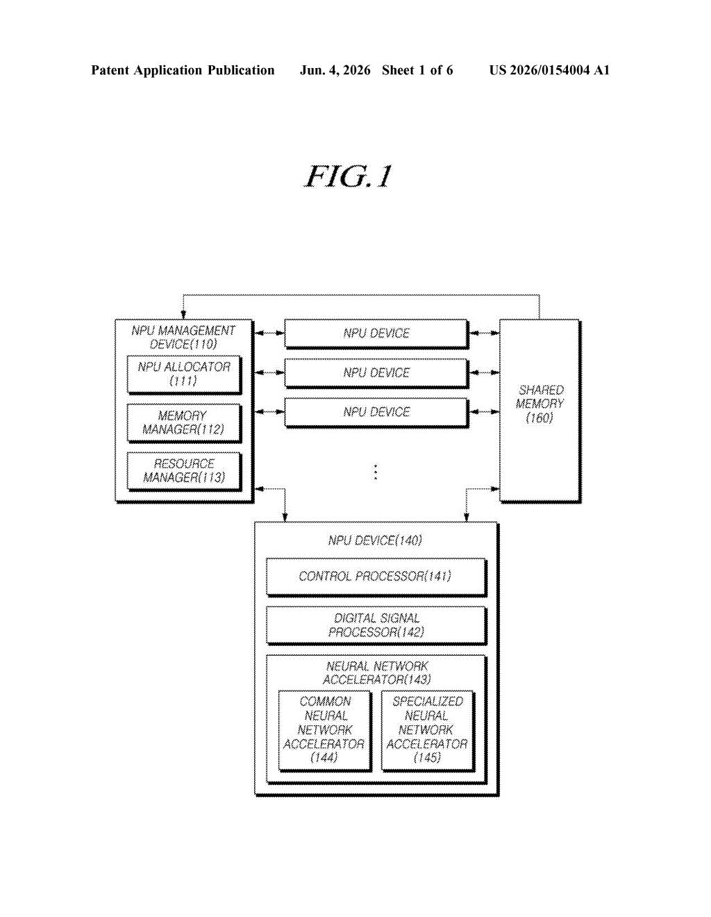
The patent describes an NPU management device (NPU stands for Neural Processing Unit — a chip designed specifically to run AI models fast and efficiently) that oversees a fleet of multiple NPUs inside a single device.
The core logic works like a smart traffic controller:
- The management layer checks whether the input or output data of an AI task is shared — meaning more than one NPU needs to read or write it.
- It then checks whether a shared memory region is currently available and not already oversubscribed.
- If both conditions are true, the data is routed into that shared pool, where every relevant NPU accelerator can access it directly without redundant copies.
The neural network accelerators referenced in the claim are the individual compute engines within each NPU device — think of them as the workers, while the NPU device is the department, and the management layer is the operations manager allocating the warehouse (shared memory).
This is a fairly targeted optimization: it doesn't change how the AI models themselves run, it just cuts down on unnecessary memory traffic when multiple accelerators are processing parts of the same workload.
What this means for on-device AI in Samsung hardware
As Samsung packs more dedicated AI silicon into its chips — the way its Exynos and mobile SoC lineup has been trending — coordinating memory access between those units becomes a real bottleneck. Without a scheme like this, each NPU might maintain its own copy of shared data, burning memory bandwidth and slowing down the whole pipeline. This patent is basically Samsung building the traffic-management infrastructure for a multi-NPU future.
For you as a user, this kind of optimization is invisible — but it's the sort of thing that determines whether your phone can run two or three AI features simultaneously without draining the battery or lagging. It's unglamorous plumbing, but plumbing matters.
This is solidly useful infrastructure work, not a flashy AI capability. Samsung is clearly planning for devices with multiple discrete NPU blocks — probably on-chip, possibly across chiplets — and this patent locks in one approach to the memory coordination problem those designs create. It's not exciting on its own, but it signals a real architectural direction.
Get one Big Tech patent every Sunday
Plain English, intelligent commentary, no hype. Free.
Editorial commentary on a publicly published patent application. Not legal advice.