Samsung Patents an Active Interconnect Die That Connects Stacked Memory to Processors
Samsung is patenting a way to wire up multiple stacks of memory chips — sitting at different distances from a processor — inside a single semiconductor package, using an active die that handles the signal routing itself.
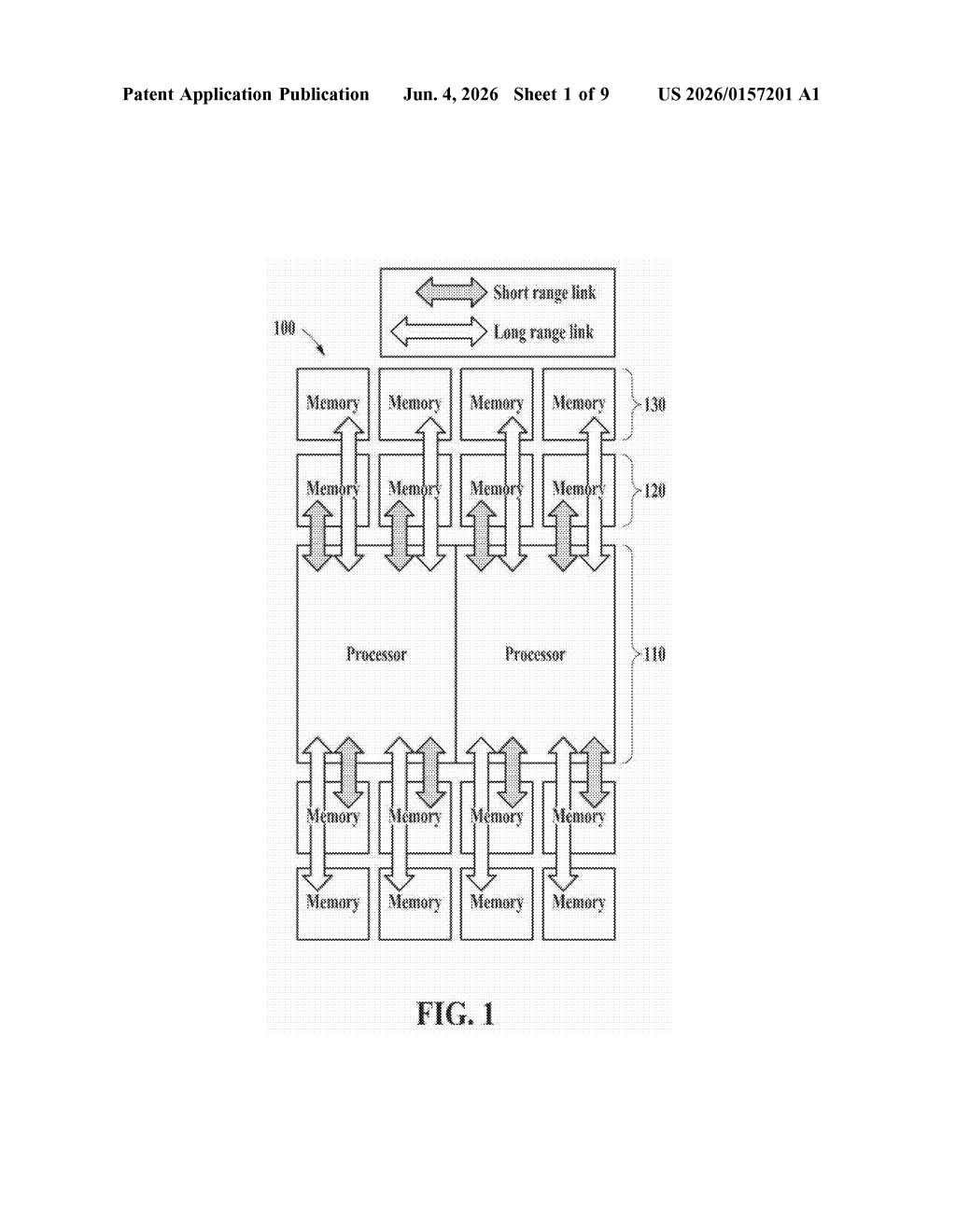
What Samsung's active interconnect die actually does
Imagine a tiny city block where a processor sits in the middle and rows of memory chips are arranged around it — some close, some farther away. The farther chips have a harder time sending data quickly because the electrical signal degrades over longer distances. That's a real engineering headache in modern chip packaging.
Samsung's patent describes a solution: a special active interconnect die that sits beneath everything else and takes responsibility for managing data traffic between the processor and all those memory stacks. Think of it as a smart traffic layer built into the foundation.
The key ingredient is a built-in modulator — a circuit that can reshape or boost signals — specifically to help the more distant memory stacks communicate reliably with the processor. It's the kind of low-level plumbing that nobody talks about but that makes high-performance chips possible.
How the modulator routes data across mismatched memory distances
The patent describes a semiconductor package with a layered architecture. At the base is the active interconnect die, which is not a passive routing slab but an active component containing a modulator and dedicated metal lines.
On top of that die sits:
- A processor die — the main compute element
- First memory dies — stacked chips positioned closer to the processor (smaller lateral distance)
- Second memory dies — stacked chips positioned farther from the processor (larger lateral distance)
The critical engineering detail is that the first metal lines in the active interconnect die are specifically designed to carry data between the farther second memory dies and the processor. That distance matters because longer on-package traces introduce signal integrity problems — resistance, capacitance, and timing skew all get worse.
The modulator (a circuit that can encode, reshape, or amplify signals — think of it as a signal conditioning unit) is presumably what compensates for that degradation on the longer paths. By making the interconnect layer active rather than passive, Samsung bakes the fix into the package itself rather than relying on the processor or memory controllers to compensate.
What this means for high-bandwidth memory packaging
High-bandwidth memory packaging — the kind used in AI accelerators, data center GPUs, and HBM (High Bandwidth Memory) stacks — lives and dies on how efficiently data moves between compute and memory inside a single package. As chipmakers cram more memory stacks into one package, the physical distance problem gets worse. An active interconnect die that handles signal conditioning internally could allow denser, more asymmetric memory layouts without sacrificing bandwidth or reliability.
For Samsung, this fits directly into its competitive push in the HBM and advanced packaging market, where it competes with SK Hynix and Micron for AI chip supply contracts. Whether this approach appears in a future HBM generation or a custom 2.5D/3D package for a hyperscaler customer isn't clear from the patent alone — but the architecture it describes is squarely aimed at that market.
This is a solid, focused piece of packaging engineering — not flashy, but the kind of work that separates competitive HBM suppliers from each other. Samsung filing this now, as the AI hardware buildout drives demand for denser memory-on-package solutions, is well-timed. The canceled claims are a red flag for the patent's legal standing, but the underlying technical idea is real and relevant.
Get one Big Tech patent every Sunday
Plain English, intelligent commentary, no hype. Free.
Editorial commentary on a publicly published patent application. Not legal advice.