
Xilinx Files Patent for On-Chip Data Format Conversion That Feeds AI Models Faster
Xilinx has patented a way to convert numeric data formats directly inside a chip's processor, skipping the software step that usually happens before AI workloads can run.
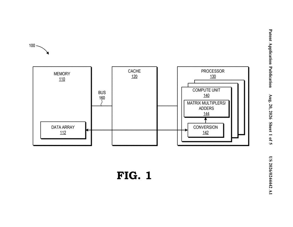
What Xilinx's on-chip format conversion actually does
AI chips are picky about the shape of data they receive. When data arrives in one numeric format but the chip's AI engine expects another, something has to translate between them, and today that translation usually happens in software, burning time and energy before any actual AI work gets done.
Xilinx's patent describes a conversion circuit built right into the processor. Feed it data in one format, tell it the size of each element in the data, and it unpacks and converts everything on the spot using a lookup table (essentially a pre-built cheat sheet of answers). The converted data goes straight to the AI compute units without an extra software step.
In practical terms, this is about cutting the overhead cost of supporting many different numeric formats, especially as AI models increasingly use compact, lower-precision numbers to save power and memory.
… converting, at conversion circuitry of the parallel processor, the input data array into an output data array in a target format based on an instruction specifying an element size in the input data array …
Translation: Specialized hardware directly reshapes data formats inside the processor based on exact size instructions.
How the LUT-based conversion pipeline works inside the chip
The patent describes a parallel processor (the kind used for AI workloads, where many calculations run at once) that includes dedicated conversion circuitry alongside its compute units.
When the processor pulls a block of data from memory, an instruction tells the conversion circuitry what element size to expect, meaning how many bits each individual number occupies. That matters because modern AI work uses many different numeric precisions: 8-bit integers, 16-bit floats, even 4-bit formats. The circuitry first unpacks the raw data by splitting it according to that element size, then passes the unpacked values through a look-up table (LUT), a hardware structure that stores pre-computed mappings so that converting one value type to another is a single fast table read rather than a chain of arithmetic.
The output of the LUT is an array in the target format that the AI compute units can immediately consume. The key claim is that the element size comes from a software instruction, making the same hardware adaptable to different format pairs without redesigning the chip.
- Data arrives from memory in an initial format
- Conversion circuitry unpacks it based on a per-instruction element size
- A LUT maps unpacked values to the target format
- AI compute units run their operations on the converted array
… employing a look up table (LUT) and the unpacked data to convert to the output data array in the target format …
Translation: The system uses a built-in reference table to quickly translate the unpacked data into the final format.
What this means for AI chip efficiency and data prep
Format conversion is invisible to users but expensive on hardware. As AI models shrink their numbers to save power (a trend called quantization), chips have to handle a growing zoo of numeric types. Doing that conversion in software adds latency and ties up the main processing resources; doing it in fixed hardware is fast but inflexible. The Xilinx approach tries to split the difference: dedicated circuitry that is still programmable because the element size comes from an instruction.
Xilinx, now part of AMD, makes the FPGAs and adaptive chips that often sit at the edge of data centers and embedded systems, where power and speed constraints are tight. A conversion mechanism that costs less than a software pass could matter a lot in those settings. The filing fits a broader pattern of chip architects trying to absorb data-prep work into silicon rather than software, a trend well represented among the latest Big Tech patents covering AI accelerator design.
AMD's new filing is the 30th we've tracked since May in our AI chip wars watchlist, adding to work like a two-table AI math shortcut and faster AI math across GPU units.
Letting software instructions decide the data size gives the chip real flexibility, but it puts serious responsibility on the code that generates those instructions. A wrong instruction corrupts the data before any conversion table even gets a chance to run.
The conversion tables themselves have a hard limit: they can only hold so many recipes before the chip's memory fills up. That is fine for today's common number formats, but gets tight as new ones keep arriving.
This design makes sense for AI systems where the software is reliable and the number formats are few and stable. The catch is that its biggest strength and its biggest weakness are the same thing.
There are more where this came from
We read every patent application Big Tech publishes and send you the ones worth knowing. Plain English, free, every week.
The drawings
5 drawing sheets from US 2026/0244442 A1 · click any drawing to enlarge


Want this weekly breakdown for a company we don't cover? Patentlyze Pro →
Be the first to weigh in