
Meta Files Patent for AR Glasses Display With Tiny Processors Built Directly Behind It
Meta's patent application says the biggest power drain in a tiny AR display is shipping the picture to it. Its fix is to build a grid of small processors right under the pixels.
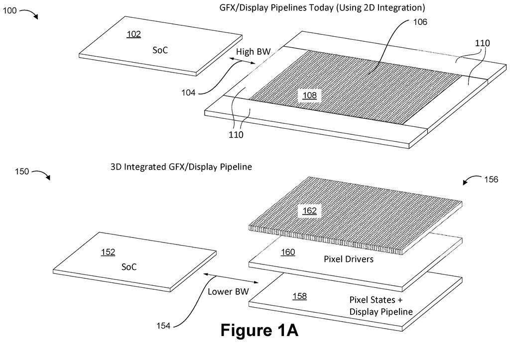
What Meta's stacked AR display actually does
You're wearing AR glasses on a long walk, and the battery icon keeps sliding down. A big share of that drain can come from moving image data from the main chip to the screen, over and over, every frame. Meta's filing says that data movement can eat about 90% of display power in some systems.
This patent application moves some of the work into the display itself. Under the pixels sits a grid of small processors, each in charge of one patch of the screen. The main chip sends the picture over, it gets split into patches, and every patch is handled at the same time, right where it will be shown.
The parts are stacked like a sandwich: processing at the bottom, pixel drivers in the middle, pixels on top. That also tucks the edge circuitry underneath, so the frame around the picture can shrink, which matters for something that has to sit on your face.
… dividing the image data into a set of tile data corresponding to different portions of the pixel array; and concurrently processing, via the plurality of compute tiles, the set of tile data …
Translation: The glasses chop up each video frame and process the pieces at the same time using stacked processors.
How each screen patch gets its own processor
The core of the claims is a display with its own small processors, called compute tiles, stacked directly with the pixel array. A frame of image data arrives and gets split into pieces (tile data), and each piece goes to a different tile. The tiles all work at the same time, and each one drives only its own patch of pixels.
Inside each tile, the data goes through a few steps:
- Gamma correction, which adjusts brightness values so they look right to the eye
- Resizing the data to fit
- Conversion to a pulse-width modulation (PWM) signal, which sets a pixel's brightness by how long it stays on
The description lays out three layers: a digital chip at the bottom, an analog chip in the middle that drives the pixels, and the display chip on top. Vertical connections called through-silicon vias link the bottom two, and hybrid bonding (a way of fusing chips face to face) joins the top two. Each tile stores its patch of the picture in its own memory as a frame buffer. In one example, a 44 by 44 grid of tiles each covers 64 by 64 pixels.
The filing also describes two add-ons. A tag-based check skips memory reads that would change nothing, saving more than 4x energy in its example. A pixel-shifting circuit nudges the image several times per frame to follow eye movement, moving only on/off states instead of full brightness values.
A method of displaying images at an electronic device having a display including a pixel array and a plurality of compute tiles stacked with the pixel array.
Translation: The patent describes tiny computer chips built directly behind the screen to help show images.
What this means for AR glasses battery life
If you wear AR glasses, the screen is one of the places where battery life and bulk get decided. Moving less image data could mean longer use between charges, and moving edge circuitry under the picture could mean a thinner border around it. The filing puts that edge circuitry at about 58% of a conventional display's footprint, and about 14% in the stacked version.
This is a patent application, so none of it is a product. Still, the target is clear: displays for AR glasses, with VR headsets, car head-up displays and camera viewfinders listed as other uses. Meta also says the design could allow richer color depth and up to about twice the frame rate.
Meta's 78th filing we've tracked since May in smart glasses work follows a swappable display module and drop-resistant lenses, adding another piece to how the company is designing these devices.
Stacking three chips into one tower costs manufacturing effort, because the layers have to be joined with tiny vertical connections. It also puts more electronics into a small space, and the filing itself names heat as one factor in choosing what to relocate under the screen. Each patch of the screen needs its own memory too, so bigger patches mean more storage and smaller ones mean more traffic between neighbors.
For glasses, that bill is worth paying. The filing says moving less data off-chip could save up to about 11% of system power, and up to about 50% with further design work, and wearers feel battery life and frame size every day. The catch is that the 50% figure depends on that extra work, and the filing shows no finished device to test it on.
Get our take in your Top Stories
Liked this breakdown? Add Patentlyze as a preferred source on Google, and our plain-English take shows up more often in your Top Stories the next time Meta patent news breaks.
There are more where this came from
We read every patent application Big Tech publishes and send you the ones worth knowing. Plain English, free, every week.
The drawings
13 drawing sheets from US 2026/0331036 A1 · click any drawing to enlarge


Show the other 5 sheets


Want this weekly breakdown for a company we don't cover? Patentlyze Pro →
Be the first to weigh in