Samsung Patents a Microscopic Surface Structure That Cools Devices Without Using Any Power
Samsung is exploring a way to cool — or heat — a device without a fan, a pump, or a single watt of electricity, using a surface covered in microscopic structures that interact with invisible heat radiation.
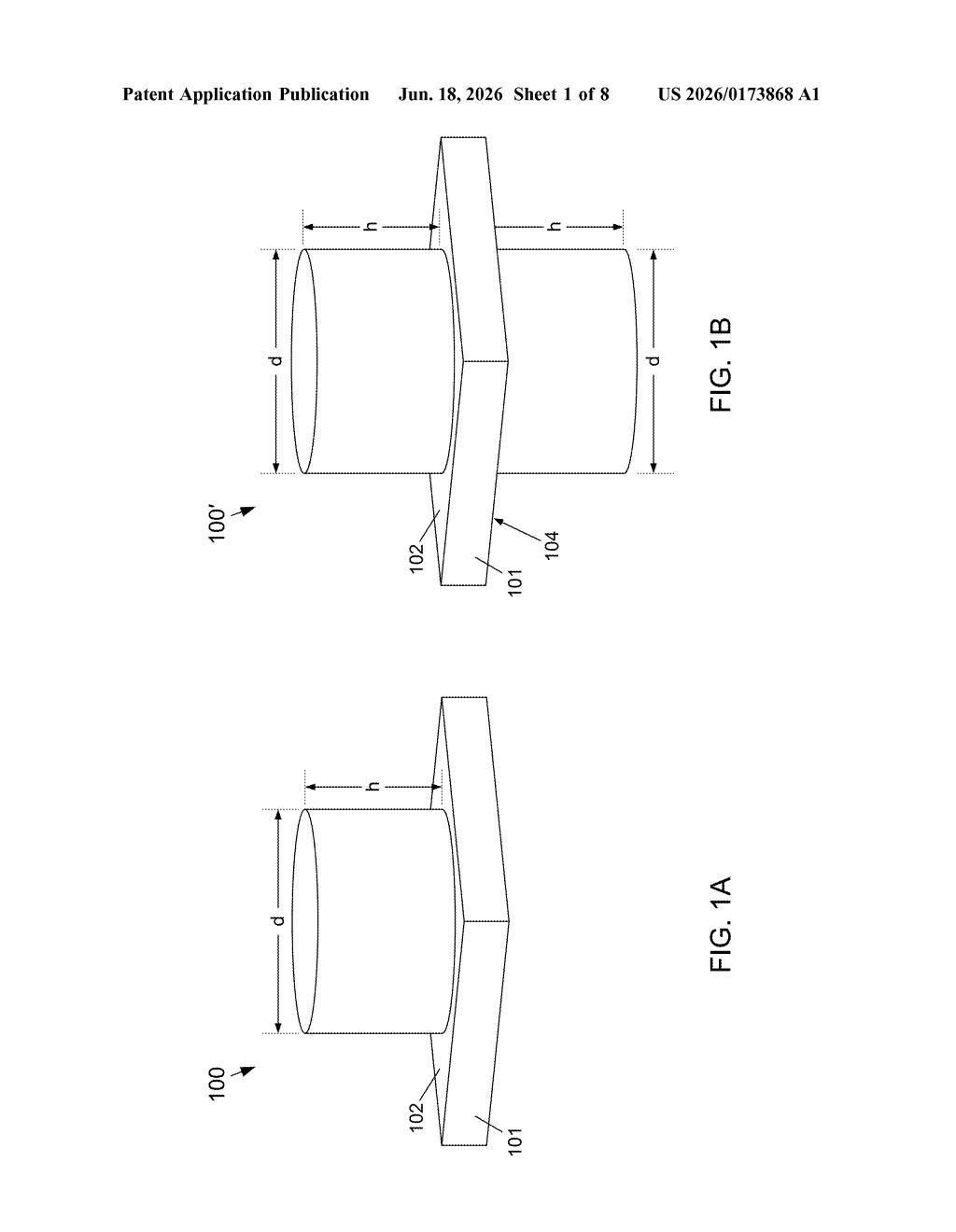
How Samsung's nanostructure coating passively manages heat
Imagine a phone or a chip that stays cool simply because of the texture of its outer surface — no fan spinning, no liquid cooling loop, no extra power draw at all. That's the core idea here.
Samsung's patent describes a surface coated with tiny structures — far smaller than a human hair — arranged in a precise pattern. Depending on the material used, these structures can either emit heat outward as invisible infrared radiation (cooling the device) or let that radiation pass through (useful for other heating or sensing applications). The structures are tall relative to their width, which is the key geometric trick that makes the effect work.
This is called "radiative passive cooling" — the same basic phenomenon that lets the night sky feel cold even on a warm evening, because heat radiates away into the atmosphere. Samsung wants to engineer that effect deliberately into device surfaces, potentially reducing how hard cooling systems have to work.
How the nanostructure geometry controls infrared emission
The patent covers two related configurations of a nanostructure device — essentially a substrate (a base material, like glass or a chip surface) with a dense, uniform array of tiny pillars or posts grown on top.
The first configuration uses materials with a low refractive index (a measure of how much a material bends and interacts with light — lower means it interferes less). These structures let more than 80% of mid-infrared radiation pass straight through, making them useful as transparent windows for infrared sensors or thermal management layers that don't absorb unwanted heat.
The second configuration — covered in the main claim — uses materials with a higher refractive index (greater than 1.75). These structures are designed to emit infrared radiation efficiently: the patent specifies an emissivity above 45% in the 8,000–13,000 nanometer wavelength range. That range sits inside the "atmospheric window," a band of wavelengths that passes through Earth's atmosphere almost unimpeded, meaning heat can radiate directly out to the cold of space:
- Each nanostructure has a height-to-width ratio of at least 1:1 (taller than it is wide)
- Structures are spread uniformly across the surface to maximize coverage
- No moving parts, no electrical input — the cooling is purely radiative
The geometry of the structures is what drives the performance: tall, slender pillars interact with infrared wavelengths in ways that flat surfaces simply cannot.
What this means for electronics cooling and energy use
Thermal management is one of the hardest unsolved problems in consumer electronics and data centers alike. As chips get faster and more power-dense, getting heat out without adding bulk, noise, or power consumption becomes a genuine engineering constraint. A passive coating that improves radiative heat loss — even modestly — could reduce the load on active cooling systems in phones, laptops, or server racks.
For Samsung specifically, this is relevant across its entire product line: smartphones, televisions, semiconductor fabrication equipment, and data center chips. The patent is early-stage and describes a materials-science foundation rather than a finished product, but it signals that Samsung is exploring radiative cooling as a real engineering tool, not just a research curiosity.
This is a legitimate materials-science patent, not a feature announcement. Passive radiative cooling is a real and active area of research, and Samsung filing here suggests it's moving from academic interest toward potential product integration. Don't expect to see "nanostructure cooling" on a spec sheet soon, but the underlying physics is sound and the engineering payoff — free cooling with no power draw — is genuinely worth pursuing.
Get one Big Tech patent every Sunday
Plain English, intelligent commentary, no hype. Free.
Editorial commentary on a publicly published patent application. Not legal advice.