
Nvidia Patents an AI That Spots Circuit Congestion Problems Before Designs Are Finalized
Every chip is essentially a tiny city, and bad urban planning during the design phase can slow the whole thing down. Nvidia is filing a patent for an AI that spots those traffic jams before anyone has committed to a layout.
What Nvidia's chip-congestion prediction actually does
Every time you tap your phone awake, three chips negotiate who runs the screen. Those chips are themselves cities of billions of tiny components, and fitting them together without creating traffic jams in the wiring is one of the hardest problems in electronics engineering.
Nvidia's patent describes a system that uses a machine learning model to predict where those traffic jams, called congestion, will form before the design is finalized. Feed in a rough map of where components might go, and the AI scores each zone of the chip for how crowded its wiring will get. Designers can then shuffle things around while there's still room to maneuver.
Right now, catching congestion problems usually means running slow, expensive simulations late in the design cycle, when fixing them is painful. This approach tries to surface the warnings much earlier, using a graph that captures how components relate to each other spatially.
… generating a graph based at least on the identified placement data, wherein one or more nodes of the graph correspond to a respective cell of the plurality of cells …
Translation: It builds a network map where each point represents a component of the chip.
How the graph model scores each region before placement
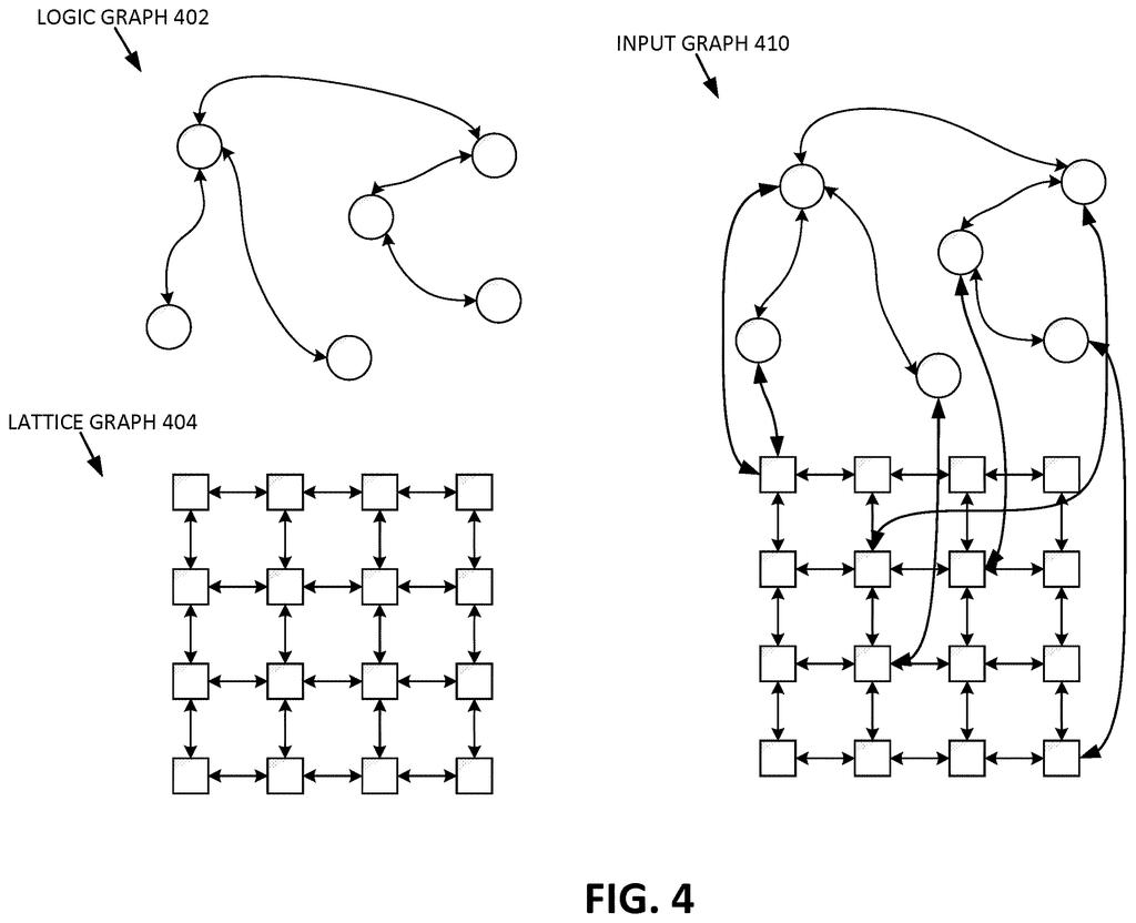
The system takes placement data for the cells (the individual logic units) of an integrated circuit and converts it into a graph, a mathematical structure where each node represents one cell and the edges capture spatial relationships between them. That graph is fed into a machine learning model.
The model was trained to look at a graph like this and predict a congestion level for specific zones called bounding areas (rectangular regions that fence in a cluster of cells). Congestion here means how packed the wiring channels in that region will become once everything is routed, which affects timing, heat, and manufacturability.
Once the model returns its predictions, the software uses that congestion score to guide where cells actually get placed. A zone flagged as high-congestion can have cells redistributed before routing even starts.
- Input: initial placement locations for cells, encoded as a graph
- Model output: congestion score per bounding area
- Action: cells are relocated based on those scores, reducing downstream routing problems
The machine learning model is trained to predict, based at least on a given graph associated with cells according to a respective IC design, a congestion level for cells at one or more bounding areas of a respective IC design.
Translation: The AI learns to forecast where circuit traffic jams will happen by analyzing the map.
What this means for the chips inside your next device
Chip design is one of the most expensive engineering processes on earth, and late-stage congestion fixes can add weeks and millions of dollars to a tape-out cycle. A model that flags problem zones early, during placement rather than after routing, could meaningfully shorten that cycle.
For everyday consumers, chips that are designed more efficiently tend to run faster and use less power. Nvidia's long bet on AI-assisted chip design shows up across several recent filings, and this patent fits squarely in that direction. The practical payoff would be chips that hit the market faster and with fewer performance compromises baked in from layout mistakes.
Nvidia's 44th filing we've tracked since July in our AI chip race watchlist, it follows one that halves AI math steps and one running two networks at once.
Claim 1 is broad in an interesting way. It covers any method that takes placement data, converts it to a graph, feeds that graph to a trained machine learning model, gets a congestion score per bounding area, and uses that score to place cells. The claim doesn't specify the architecture of the ML model, the size of the chip, or the exact graph construction method. That breadth means Nvidia is staking territory across a wide swath of AI-guided placement pipelines, not just one specific implementation.
In practice, if granted, claim 1 could apply to almost any EDA (chip design software) tool that adds an ML congestion predictor to its placement loop, which is a real and growing category. Whether the claim survives prior-art scrutiny is another question entirely, but the coverage it's reaching for is wide.
For a general reader, the honest summary is this: Nvidia is trying to own a key step in the AI-assisted chip design workflow at a fairly abstract level. That's a commercially significant position to hold, because faster, cheaper chip design benefits every product that contains a chip.
There are more where this came from
We read every patent application Big Tech publishes and send you the ones worth knowing. Plain English, free, every week.
The drawings
10 drawing sheets from US 2026/0289339 A1 · click any drawing to enlarge


Want this weekly breakdown for a company we don't cover? Patentlyze Pro →
Be the first to weigh in