
Samsung Patents a Self-Grounding PCB Mount for Display Devices
Samsung has filed a patent for a display device where the circuit board grounds itself to the chassis the moment it's physically mounted — no separate grounding step, no extra hardware.
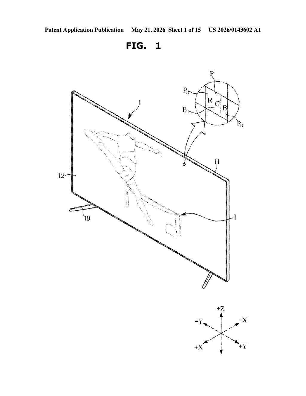
What Samsung's integrated PCB grounding actually does
Imagine building a TV or monitor and needing to make sure the circuit board inside is properly grounded — meaning safely connected to the metal frame so stray electrical charges don't cause interference or damage. Normally, that involves an extra step: a separate wire, a screw, or a grounding clip that someone has to attach deliberately.
Samsung's patent describes a simpler approach. The printed circuit board has a small protruding tab — the 'grounding portion' — built right into it. When you snap the board into its slot on the chassis, that tab automatically presses against the metal frame and makes the grounding connection. No separate parts, no extra assembly step.
It's a small but real quality-of-life improvement for display manufacturing. Fewer parts means fewer things that can be missed, misinstalled, or fail over time. The idea is elegantly boring — which is often the hallmark of a genuinely useful engineering fix.
How the grounding portion contacts the chassis on mount
The patent describes a display device — think a TV, monitor, or flat-panel screen — made up of three key components working together.
- Display panel: the screen itself.
- Chassis: the metal structural frame that surrounds and supports the panel, which includes a dedicated board mounting portion — a specific area designed to accept a circuit board.
- Printed circuit board (PCB): the electronics board, which has two key features: a coupling portion that physically attaches to the board mounting area, and a grounding portion — a small protrusion on the surface of that coupling section.
The clever bit is in the geometry. The grounding portion is sized and positioned so that when the PCB is seated into the chassis mount, that protrusion is automatically pressed into contact with the chassis metal. This creates the electrical ground connection (a low-resistance path that drains unwanted charge) as a direct consequence of the mechanical assembly, rather than as a separate step.
In manufacturing terms, this collapses two operations — mounting and grounding — into one, which reduces assembly time and eliminates a category of potential assembly errors.
What this means for display assembly and reliability
For Samsung's display manufacturing lines, this kind of incremental simplification adds up. Displays are produced at enormous scale, and any reduction in assembly steps, parts count, or potential failure points translates directly into cost and reliability improvements. A grounding failure that causes EMI (electromagnetic interference) or component damage is an expensive warranty issue — this approach makes that failure mode harder to introduce in the first place.
For end users, you'd never notice this directly — but you might benefit from it indirectly through fewer dead-on-arrival units or longer display lifespan. It's the kind of unsexy engineering detail that separates high-volume consumer electronics from cheaper alternatives.
This is a routine manufacturing optimization patent — there's no new science here, just a tidy mechanical design that merges two assembly steps into one. It's not something that will generate headlines, but it's exactly the kind of incremental IP that Samsung files by the thousands to protect its manufacturing process know-how. If you're covering Samsung's display hardware strategy, it's a footnote, not a story.
Get our take in your Top Stories
Liked this breakdown? Add Patentlyze as a preferred source on Google, and our plain-English take shows up more often in your Top Stories the next time Samsung patent news breaks.
There are more where this came from
We read every patent application Big Tech publishes and send you the ones worth knowing. Plain English, free, every week.
Want this weekly breakdown for a company we don't cover? Patentlyze Pro →