
Samsung Patents a Way to Decrypt Data Inside the Memory Chip Itself
Every time your phone reads protected data from memory, that data has to travel across a bus and get decrypted before it can be used, a tiny tax paid millions of times a second. Samsung's new patent proposes moving the decryption step directly into the memory chip, cutting out that round trip entirely.
What Samsung's in-memory decryption actually does
Right now, the memory chips inside your phone store encrypted data and ship it out in locked form. A separate part of the main processor then has to unlock it before anything useful can happen, which means more data moving across more wires, burning more power, every single time.
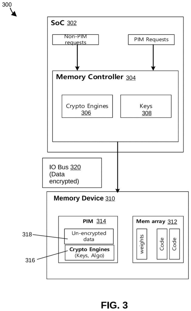
Samsung's patent describes memory chips with a built-in cryptographic engine, essentially a tiny decoder that lives right where the data is stored. Encrypted data comes in over the memory bus, gets unlocked on the spot, and is ready to use without ever making that extra trip to the processor.
The patent pairs this with Processing-in-Memory (PIM) technology, which lets the memory chip do some computing on its own rather than always handing work back to the main processor. Together, the two ideas could mean your phone does more work with less energy, which matters most when you're running demanding apps on battery.
A memory device comprising a cryptographic engine (CE), wherein the memory device is configured to receive encrypted data via a memory input/output (IO) bus, and wherein the CE is configured to decrypt the encrypted data to obtain decrypted data.
Translation: The chip has a built in security engine that decrypts incoming data right inside the memory.
How the cryptographic engine sits inside the memory device
The patent describes a memory device (the kind of chip that stores data in a mobile phone or tablet) that includes a built-in cryptographic engine (CE). Normally, encrypted data travels across the memory I/O bus (the data highway between memory and processor) in locked form, and decryption happens elsewhere on the chip. Here, the CE sits inside the memory device itself and handles decryption before the data goes anywhere.
The system works alongside Processing-in-Memory (PIM) or Processing-Near-Memory (PNM) units. PIM means compute logic is embedded directly in the memory array; PNM means it sits just outside the memory array but still within the memory package. Either way, the goal is the same: let the memory chip do real computational work on data that has already been decrypted locally, rather than shipping raw encrypted bytes to the main processor for every operation.
The flow the patent describes looks like this:
- Encrypted data arrives at the memory device over the I/O bus.
- The cryptographic engine decrypts it inside the memory chip.
- The PIM or PNM unit processes the now-decrypted data on the spot.
- Results go back to the main processor or to other parts of the system.
The architecture targets mobile Systems-on-a-Chip (SoCs), meaning the integrated chips that run smartphones and tablets, where power efficiency and thermal limits are tight constraints.
The memory device can further comprise a PIM or PNM device configured to process the decrypted data.
Translation: Once unlocked inside the chip, the data goes straight to a processor for immediate work.
What this means for mobile chip power and speed
Moving decryption into memory reduces the volume of raw encrypted data that has to travel across the chip's internal bus. That matters because bus traffic is one of the hidden drains on battery life and processing speed in mobile devices. If the memory chip can handle both decryption and some computation locally, the main processor gets a lighter workload and the whole system does more per milliwatt.
The practical upside is modest but real: phones that stay cooler, last longer on a charge, or handle data-heavy tasks (like on-device AI processing) more efficiently. Samsung is one of the world's largest memory chip makers, so a patent like this reflects exactly the kind of chip-level integration that shows up across new tech patents covering mobile memory and SoC architecture right now.
That makes this Samsung's 41st filing we've tracked since June in the AI chip wars, a list that already includes one on math inside memory and one on signal tunnels in chips.
Every time a phone handles encrypted data, that data has to travel off the memory chip to be decoded, then travel back. On a phone running a camera filter or an AI assistant on battery, that round trip happens constantly, burning power and slowing things down in ways users notice as heat and lag.
Samsung's approach moves the decoding step onto the memory chip itself, so the data never has to leave. That removes a real bottleneck, and the efficiency gains scale with how often the phone handles sensitive data, which on a modern device is nearly always.
The gap between a patent filing and a phone on a shelf is wide, and this document covers the concept, not the engineering detail needed to ship it. But the problem it targets is genuine and growing, as phones take on tasks that once required a desktop.
Get our take in your Top Stories
Liked this breakdown? Add Patentlyze as a preferred source on Google, and our plain-English take shows up more often in your Top Stories the next time Samsung patent news breaks.
There are more where this came from
We read every patent application Big Tech publishes and send you the ones worth knowing. Plain English, free, every week.
The drawings
15 drawing sheets from US 2026/0254641 A1 · click any drawing to enlarge


Want this weekly breakdown for a company we don't cover? Patentlyze Pro →
Be the first to weigh in