
Samsung Patents a Water-Based Method for Depositing Chip-Grade Molybdenum Films
Samsung has filed a patent for a method of building ultra-thin molybdenum metal films on a chip substrate one atomic layer at a time, using ordinary water as the key chemical ingredient to do the converting.
What Samsung's molybdenum film process actually does
A chip factory prints millions of microscopic features onto a silicon wafer every day. Each of those features might require an extremely thin layer of metal, and getting that metal to sit perfectly flat and uniform is one of the hardest parts of the whole operation.
Samsung's patent describes a process for doing exactly that with molybdenum, a metal valued in chip-making for its high conductivity and heat resistance. The method works like painting a wall one paper-thin coat at a time: you spray on a molybdenum-containing chemical, clear the air, spray on water to trigger a reaction that locks the metal in place, then clear the air again. Repeat until you have the thickness you need.
The surprising part is the role of water. Most processes like this use harsh hydrogen gas or other aggressive chemicals to do the converting step. Using water (H2O) as the reducing agent is a gentler, potentially safer approach that Samsung is betting can still produce a high-quality metal film.
… supplying a reducing agent containing water (H 2 O) onto the chemisorption layer of the molybdenum precursor, thereby forming a molybdenum thin film …
Translation: Water is used to help transform the applied chemical layer into a solid molybdenum film.
How water replaces conventional reducing agents in each cycle
The patent describes a technique called atomic layer deposition (ALD), a process that builds a thin film one molecular layer at a time by cycling through a fixed set of chemical steps. Each cycle adds only a tiny amount of material, but you can repeat it hundreds of times to reach the exact thickness you want.
Here is what a single cycle looks like:
- Step 1 (Precursor injection): A molybdenum-containing gas is introduced onto the substrate, and the molecules chemically attach to the surface in what is called a chemisorption layer (essentially, the molecules grip the surface rather than just sitting on top of it).
- Step 2 (First purge): An inert gas is swept through to blow away any precursor molecules that did not bond, leaving only the tightly attached layer.
- Step 3 (Reduction with water): Water vapor is introduced. It reacts with the attached molybdenum compound and converts it into a thin layer of metallic molybdenum, releasing the oxygen or other byproducts.
- Step 4 (Second purge): Another sweep of inert gas clears the chamber before the next cycle begins.
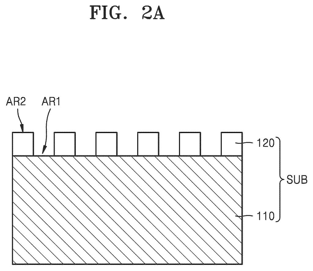
The substrate has two defined regions (a first region and a second region), suggesting the process may be designed to deposit selectively or to track uniformity across different surface areas. The cycling structure is what gives ALD its precision: each pass is self-limiting, meaning the reaction stops once all available surface sites are filled.
Provided is a method of manufacturing a molybdenum film by repeatedly performing a cycle, wherein the cycle includes preparing a substrate including a first region and a second region …
Translation: The process relies on a repeating sequence of steps applied to a base material split into two specific areas.
What this means for next-generation chip materials
Molybdenum is attracting attention in the semiconductor industry as chip designs push into tighter dimensions where traditional metals like tungsten or copper become unreliable. A controlled, repeatable ALD process for molybdenum could feed directly into logic or memory manufacturing lines without requiring a complete retooling of existing deposition equipment.
The shift to water as the reducing agent is the filing's most commercially interesting detail. Hydrogen-based reduction runs at high temperatures and carries safety overhead; a water-based route, if it produces equally pure films, could lower process complexity. Samsung's chip fabrication division and its foundry business would both have immediate use for a well-controlled molybdenum deposition recipe, and the steady stream of semiconductor-materials patents like this one sits alongside new Big Tech patents across memory, logic, and packaging that together sketch where next-generation chip manufacturing is heading.
Process chemistry filings sit about as close to the factory floor as patents get, and that's what this is. The distance to a shippable product is short in one sense: ALD equipment already exists in every advanced fab, and swapping in a new precursor-plus-water chemistry is an incremental change to a known workflow. The real gating factor is validation data: whether water reduction produces molybdenum films with resistivity and defect counts that meet production specs. Samsung publishes these process filings steadily, and this one reads like lab-to-pilot-line work rather than exploratory research.
There are more where this came from
We read every patent application Big Tech publishes and send you the ones worth knowing. Plain English, free, every week.
The drawings
25 drawing sheets from US 2026/0234796 A1 · click any drawing to enlarge


Want this weekly breakdown for a company we don't cover? Patentlyze Pro →
Be the first to weigh in