
Samsung
Samsung · Chip · Filed Mar 11, 2025 · USPTO published May 14, 2026 · May 14 release
Samsung Files Patent for Selective-Protection Semiconductor Etching Process
Deep inside a chip factory, the difference between a working transistor and a dead one can come down to a single masking step. Samsung is patenting a way to protect some circuit lines while selectively cutting others — a building block of modern chip patterning.
- Publication number
- US 2026/0136904 A1(US20260136904A1)
- Applicant
- SAMSUNG ELECTRONICS CO., LTD.
- Filed · Published
- Mar 11, 2025 · May 14, 2026
- Inventors
- Eunshoo HAN, Byeung Chul KIM
- Status when we published
- Waiting for an examiner
- Document
- 20 claims
- US classification
- 438/400
What Samsung's selective-etch chip fab method actually does
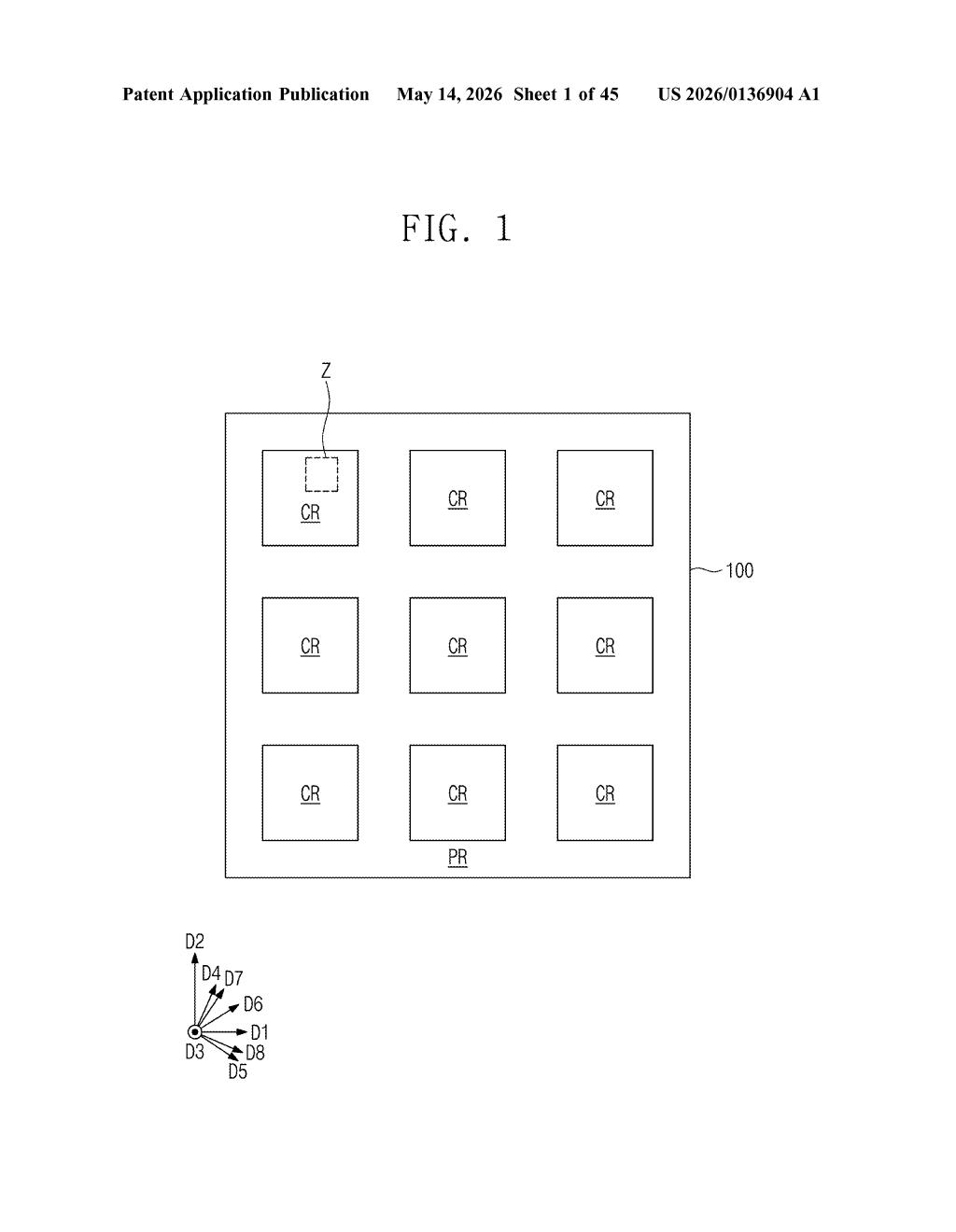
Imagine laying down a grid of tiny wires on a surface, then wanting to cut only some of them at specific points — without accidentally damaging the ones you want to keep. That's essentially the challenge Samsung is solving here with a targeted fabrication technique.
The process starts by creating two sets of parallel lines on a silicon substrate. A protection layer is then placed on just one set of lines — think of it like putting tape over the wires you don't want to cut. An etching pattern is then applied across both sets, and only the unprotected lines get cut where the pattern overlaps them.
The result is a more precise set of active patterns — the foundational structures that define where transistors and connections live on a chip. Getting these shapes exactly right is critical to making chips smaller, faster, and more energy-efficient.
How the protection pattern controls which lines get etched
The patent describes a multi-step photolithographic and etching sequence for defining active regions on a semiconductor substrate — the areas that will eventually become transistors or conductive pathways.
Here's the sequence the patent lays out:
- Step 1: Two sets of line patterns (first and second) are formed running parallel in a first direction, spaced apart from each other in a perpendicular second direction.
- Step 2: A protection pattern is selectively deposited only on the first line pattern — shielding it from the etch that follows.
- Step 3: An etching pattern is formed across both line sets, running diagonally in a third direction that crosses both prior directions.
- Step 4: The exposed portion of the second line pattern — wherever it overlaps with the etching pattern — is removed.
The key innovation is the selective nature of the protection step. By covering only one set of lines, Samsung can use a single etching pass to cut specific segments of the second line pattern without touching the first. This kind of differential masking reduces the number of separate lithography steps needed, which matters enormously at scale.
The patent falls under USPC 438/400, which covers semiconductor device manufacturing methods — a broad and highly competitive classification space.
What this means for Samsung's chip manufacturing precision
Chip fabrication at leading-edge nodes (think 3nm, 2nm) is an exercise in extreme precision. Every additional masking or etching step adds cost, time, and potential for defects. A method that achieves complex pattern differentiation with fewer steps is genuinely valuable on a production line, even if it sounds mundane from the outside.
For Samsung, which operates some of the world's most advanced fabs and competes directly with TSMC and Intel Foundry, incremental improvements in patterning efficiency compound into real yield and cost advantages. You probably won't notice this in a spec sheet — but it's the kind of foundational process IP that underpins every chip Samsung makes.
Source: US 2026/0136904 A1 at the USPTO (PDF). Full patent text and figures are in the official publication.
Get our take in your Top Stories
Liked this breakdown? Add Patentlyze as a preferred source on Google, and our plain-English take shows up more often in your Top Stories the next time Samsung patent news breaks.
Add Patentlyze on Google
One click.
There are more where this came from
We read every patent application Big Tech publishes and send you the ones worth knowing. Plain English, free, every week.
More from Samsung
All 1,629 Samsung patents →


More in Chip
All 645 Chip patents →
Sony
Sony Patents a Camera That Keeps Stabilizing Images When Its Chip Falls Behind

Sony
Sony Patents a Photon-Counting Circuit That Reduces Wasted Electrical Switching

Sony
Sony Patents a Three-Layer Camera Chip That Protects Itself from Electrical Damage
OpenAI