
Sony Files Patent for a Two-Layer Camera Chip That Is Easier to Make
Most cameras record everything, all the time. Sony's patent describes a sensor with a built-in motion watcher that can trigger a normal photo when it spots a chosen object, and it is designed to be simpler to manufacture.
What Sony's two-job camera chip actually does
Imagine a camera on a factory robot or the front of a car. Recording full-color video every second is wasteful, but a camera that watches only for movement and takes a picture when something important appears can do the job with less.
Sony's patent is about building that kind of sensor. It mixes two kinds of pixels (the tiny light-catching dots that make up a camera's image sensor) on one chip: ordinary color pixels that take pictures, and motion-watching pixels that only notice when something in view gets brighter or darker. When the motion watchers spot a chosen object, the color pixels take the shot.
The real trick is in how it is built. Sony splits the circuitry across two stacked layers so the two pixel types look nearly identical on the top layer, which should make the sensor simpler and cheaper to manufacture.
… a transfer transistor that opens and closes a path between a photoelectric conversion element and a contact is arranged among a gradation pixel that generates a gradation signal according to a light amount and a detection pixel that detects whether or not a change amount of luminance exceeds a predetermined threshold …
Translation: The top chip handles light sensing and basic switching duties.
How Sony splits the sensor across two stacked chips
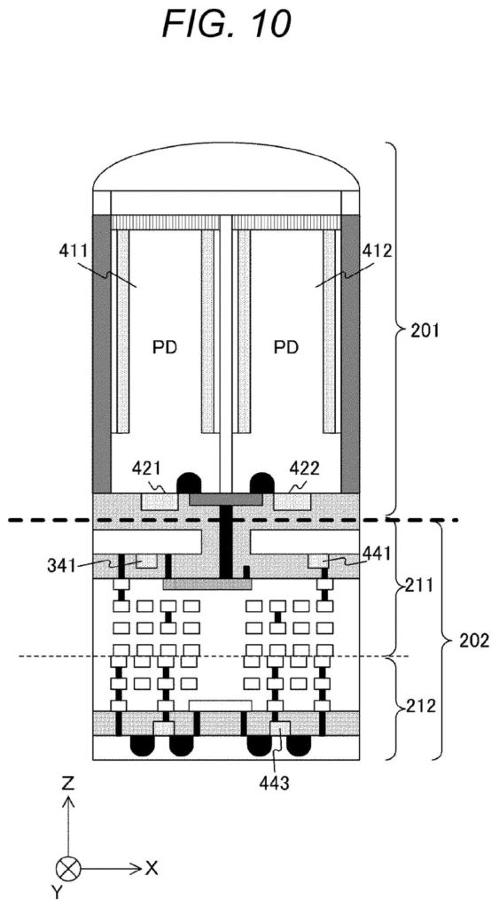
The patent covers an image sensor made of two stacked chips: a light receiving chip on top and a circuit chip underneath, joined by copper-to-copper bonds. The sensor has two kinds of pixels. Gradation pixels measure how much red, green or blue light arrives, which produces a normal picture. Detection pixels (often called event-based vision sensor, or EVS, pixels) report only whether brightness at that spot changed by more than a set threshold.
The central claim is where the electronics go. Only the transfer transistor (a tiny switch that lets charge flow from the light-catching element toward the circuits) stays on the top chip, for both pixel types. Every other transistor sits on the bottom chip. The detection circuit there works in steps:
- It turns the light current into a logarithmic voltage (a compressed scale of brightness).
- It buffers that voltage and subtracts the earlier value to find the change.
- It compares the change with upper and lower thresholds and sends out a detection signal.
Because the top chip looks the same for both pixel types, Sony says it avoids making two separate layouts. It also keeps the noisy detection circuits away from the light-collecting layer, where they could interfere with the picture signal. The filing also describes versions where the same eight light sensors switch between event mode and picture mode in turns, and one with a switching transistor removed.
Why a simpler layout matters for phones and cars
If you use a smartphone, ride in a car with driver-assist features, or work around robots, the camera is the part that has to notice things quickly. The filing names smartphones, industrial robot cameras and in-vehicle cameras as places this sensor could go. The payoff Sony claims is on the factory side: fewer manufacturing steps and a lower system cost, which often decides whether a clever sensor ends up in everyday gear.
Sony also says the layout improves image quality, since the top layer keeps its full light-collecting area. In one version, the motion-watching pixels can double as picture pixels, so more of the sensor goes toward your photos. Nothing in the filing points to a specific product. It describes a chip design.
Sony's 37th filing we've tracked since July in the self-driving sensing race, it builds on earlier applications covering pixel separation walls and a self-correcting laser sensor.
You will never see this patent in action. It adds no button, no mode and no new picture style. Its stated goal is fewer manufacturing steps for the company that makes the sensor.
Where you could feel it is downstream. A sensor that is cheaper to build could make it easier to put a motion-watching feature into a phone or a car camera. The filing also says keeping the noisy motion circuits off the top layer protects the picture signal from interference.
The verdict is a routine engineering refinement with a small payoff, mostly for Sony and its customers' budgets. If it works as described, the best outcome for you is a camera that does more for the same price and looks no different from the outside.
Get our take in your Top Stories
Liked this breakdown? Add Patentlyze as a preferred source on Google, and our plain-English take shows up more often in your Top Stories the next time Sony patent news breaks.
There are more where this came from
We read every patent application Big Tech publishes and send you the ones worth knowing. Plain English, free, every week.
The drawings
22 drawing sheets from US 2026/0352968 A1 · click any drawing to enlarge


Show the other 14 sheets


Want this weekly breakdown for a company we don't cover? Patentlyze Pro →
Be the first to weigh in