
Sony · Filed Jul 13, 2026 · Published Nov 5, 2026

Sony Files Patent for a Camera Sensor That Captures Moving Subjects Without Warping

Sony has drawn up a camera pixel that records a whole frame at once, so a spinning fan or a speeding car stays straight instead of leaning. The filing also adds a trick for stacked chips that gives tiny pixels more room to store light.
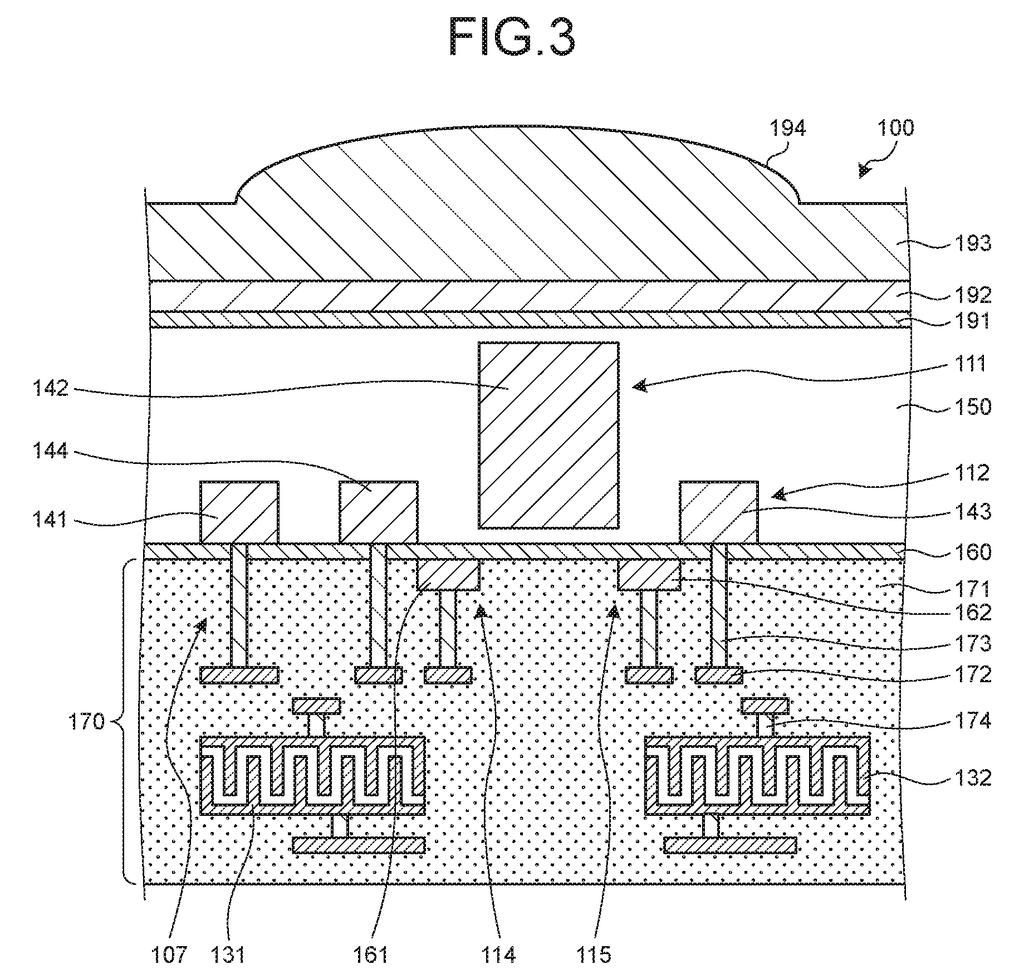
Cutaway view of a light-sensing camera element with a tiny lens and built-in electrical storage to prevent motion blur. Drawing from patent filing US 2026/0352972 A1.
Cutaway view of a light-sensing camera element with a tiny lens and built-in electrical storage to prevent motion blur.
See all 61 drawings from this filing ↓
Publication number US 2026/0352972 A1 US20260352972A1
Applicant SONY SEMICONDUCTOR SOLUTIONS CORPORATION
Filing date Jul 13, 2026
Publication date Nov 5, 2026
Inventors Yoshimichi KUMAGAI, Masashi BANDO, Naoyuki OSAWA, Shunya AKIYAMA, Toru SHIRAKATA, Takashi ABE, Tomoya AOTA
US classification 348/294
Status when we published Waiting for an examiner (Jul 28, 2026)
Parent application is a Division of 18692442 (filed 2024-03-15)
Document 18 claims

What Sony's two-memory camera pixel actually does

Ever tried to snap a photo of a spinning fan or a passing train and ended up with a bent, leaning mess? Most cameras read their sensor one row at a time, so the top of the picture is captured slightly before the bottom. Anything moving fast gets stretched out of shape.

Sony's filing describes a sensor built around a global shutter: every pixel is exposed at the same instant and holds its result until the chip is ready to read it. Each pixel keeps two small notes, a baseline reading from the start of the exposure and a reading of the actual picture. The chip subtracts one from the other, which cancels a lot of stray noise.

Sony's main tweak is the layout. It puts the reset switch right beside the spot where light is stored, so leftover charge gets cleared more completely. A second idea adds extra metal posts so tiny pixels can store more.

From the filing · CLAIM 1
… a first capacitive element that holds a level of the signal at a time of resetting by the first reset unit; a second capacitive element that holds a level of the signal when the charge is transferred to the charge holding unit; …

Translation: The sensor uses two separate storage parts to capture baseline reset levels and actual image data separately.

How the pixel stores a before and after reading

The first independent claim covers a single pixel built for a global shutter. Light hits a photodiode (a light-sensitive spot that turns light into electric charge), and the charge is moved to a charge holding unit (a small storage region, called a floating diffusion). An amplifier then turns that stored charge into a signal on a first output node.

Two capacitive elements (tiny electrical storage parts) hang off that node. One holds the signal level right after a reset, and the other holds the level once the charge has been transferred. A readout circuit later reads both and outputs them as the image signal. Comparing the two is called correlated double sampling (using a baseline reading to cancel offset errors). The description says this also reduces parasitic light sensitivity, which is stray light leaking into the stored charge.

The layout detail is that the reset unit sits directly next to the charge holding unit. The description says earlier designs kept them apart, which made it hard to drain leftover charge and added noise.

The second independent claim stacks two chip layers. A capacitance addition wiring (a metal post that passes through the upper chip) connects to the wiring of the charge holding unit and adds storage capacity. Small pixels otherwise run out of room, which narrows the range of brightness the sensor can record. Several of these posts can share one opening with other through-wiring to save space.

From the filing · THE ABSTRACT
A readout circuit is connected to a second output node, reads each of the reset level held in the first capacitive element and the image signal level held in the second capacitive element, and outputs the reset level and the image signal level as a reset signal and an image signal, respectively.

Translation: A readout circuit processes both stored levels to produce the final clean image.

Why phone-sized pixels need extra storage room

If you shoot video of kids running, a sports game or traffic, a global shutter sensor is what keeps vertical lines straight. The catch is that the extra storage parts crowd each pixel, and phones, cars and medical cameras have very little room to spare. The filing lists digital cameras, smartphones, vehicle cameras that spot pedestrians and endoscopes as places the design could apply.

The filing also reads as a pitch for shrinking sensors without hurting picture quality. The description says the stacked layout lets pixels get smaller or sharper, and that the extra wiring protects the range of brightness a pixel can record. Note that this is a divisional filing, meaning it splits off ideas from an earlier Sony application, so it is a refinement of existing work and not a new direction.

Sony's 98th filing in the Display patents we cover since May follows one on bright and dim light and one on flagging pixels to ignore.

Editorial take

Global shutter costs space. Every pixel needs two storage parts plus extra switches, so the pixel gets crowded, and crowded pixels either grow larger or catch less light. Sony's answer is to stack a second chip layer underneath and move the extras there.

That move has its own price. The metal posts that carry signals through the lower chip eat into the room left for circuits, and the extra storage posts add to the bill. Grouping several posts in one opening is a sensible way to limit the damage.

The trade reads as worth it. Warped footage of moving subjects is an obvious annoyance, and a little lost floor space is a fair price for fixing it. It is careful engineering and a modest step, and it will matter more to chip designers than to anyone holding the camera.

Get our take in your Top Stories

Liked this breakdown? Add Patentlyze as a preferred source on Google, and our plain-English take shows up more often in your Top Stories the next time Sony patent news breaks.

There are more where this came from

We read every patent application Big Tech publishes and send you the ones worth knowing. Plain English, free, every week.

The drawings

61 drawing sheets from US 2026/0352972 A1 · click any drawing to enlarge

Sensor chip layout with pixel grid and controls, drawing sheet 1 from US 2026/0352972 A1
Sheet 1 Sensor chip layout with pixel grid and controls
Wiring inside a single pixel that temporarily stores light data, drawing sheet 2 from US 2026/0352972 A1
Sheet 2 Wiring inside a single pixel that temporarily stores light data
Side view showing tiny storage capacitors embedded beneath the lens, drawing sheet 3 from US 2026/0352972 A1
Sheet 3 Side view showing tiny storage capacitors embedded beneath the lens
Folded metal layers that store more charge, drawing sheet 4 from US 2026/0352972 A1
Sheet 4 Folded metal layers that store more charge
Overhead map of light collectors in one pixel, drawing sheet 5 from US 2026/0352972 A1
Sheet 5 Overhead map of light collectors in one pixel
Exposure signals sent simultaneously to all pixels to freeze motion, drawing sheet 6 from US 2026/0352972 A1
Sheet 6 Exposure signals sent simultaneously to all pixels to freeze motion
How the sensor pulls clean data from memory, drawing sheet 7 from US 2026/0352972 A1
Sheet 7 How the sensor pulls clean data from memory
Upgraded pixel design holding signals across four capacitors, drawing sheet 8 from US 2026/0352972 A1
Sheet 8 Upgraded pixel design holding signals across four capacitors
Show the other 52 sheets
Pixel layout adding extra capacitors to prevent distortion, drawing sheet 9 from US 2026/0352972 A1
Sheet 9 Pixel layout adding extra capacitors to prevent distortion
Alternative pixel layouts arranged for larger sensor sizes, drawing sheet 10 from US 2026/0352972 A1
Sheet 10 Alternative pixel layouts arranged for larger sensor sizes
Connecting two pixels together to share readout circuits, drawing sheet 11 from US 2026/0352972 A1
Sheet 11 Connecting two pixels together to share readout circuits
Surface layout of two neighboring pixels sharing power lines, drawing sheet 12 from US 2026/0352972 A1
Sheet 12 Surface layout of two neighboring pixels sharing power lines
Two pixels arranged to share a single readout amplifier, drawing sheet 13 from US 2026/0352972 A1
Sheet 13 Two pixels arranged to share a single readout amplifier
Wiring four pixels to share common output electronics, drawing sheet 14 from US 2026/0352972 A1
Sheet 14 Wiring four pixels to share common output electronics
Layout of four pixels grouped around shared readout parts, drawing sheet 15 from US 2026/0352972 A1
Sheet 15 Layout of four pixels grouped around shared readout parts
Splitting pixel circuits across two stacked silicon chips, drawing sheet 16 from US 2026/0352972 A1
Sheet 16 Splitting pixel circuits across two stacked silicon chips
Two stacked silicon layers separating light sensing from memory, drawing sheet 17 from US 2026/0352972 A1
Sheet 17 Two stacked silicon layers separating light sensing from memory
Vertical connectors linking the top sensor to lower memory cells, drawing sheet 18 from US 2026/0352972 A1
Sheet 18 Vertical connectors linking the top sensor to lower memory cells
Separate chip layouts for light detection and signal storage, drawing sheet 19 from US 2026/0352972 A1
Sheet 19 Separate chip layouts for light detection and signal storage
Added overflow gates prevent bright light from bleeding into pixels, drawing sheet 20 from US 2026/0352972 A1
Sheet 20 Added overflow gates prevent bright light from bleeding into pixels
Rearranged lower storage circuits with shared ground connections, drawing sheet 21 from US 2026/0352972 A1
Sheet 21 Rearranged lower storage circuits with shared ground connections
Grouping four adjacent pixels to share common readout parts, drawing sheet 22 from US 2026/0352972 A1
Sheet 22 Grouping four adjacent pixels to share common readout parts
Detailed top view of a single pixel layout, drawing sheet 23 from US 2026/0352972 A1
Sheet 23 Detailed top view of a single pixel layout
Internal wiring that holds analog signals before digital readout, drawing sheet 24 from US 2026/0352972 A1
Sheet 24 Internal wiring that holds analog signals before digital readout
Transistor layouts arranged to fit within a single pixel, drawing sheet 25 from US 2026/0352972 A1
Sheet 25 Transistor layouts arranged to fit within a single pixel
Side by side versus stacked layouts for camera processing chips, drawing sheet 26 from US 2026/0352972 A1
Sheet 26 Side by side versus stacked layouts for camera processing chips
Cross section of a single-chip sensor with built-in processing, drawing sheet 27 from US 2026/0352972 A1
Sheet 27 Cross section of a single-chip sensor with built-in processing
Cross section of two stacked sensor layers bonded together, drawing sheet 28 from US 2026/0352972 A1
Sheet 28 Cross section of two stacked sensor layers bonded together
Pixel array split across two stacked semiconductor wafers, drawing sheet 29 from US 2026/0352972 A1
Sheet 29 Pixel array split across two stacked semiconductor wafers
Internal wiring between stacked pixel and readout layers, drawing sheet 30 from US 2026/0352972 A1
Sheet 30 Internal wiring between stacked pixel and readout layers
Alternative vertical connections between stacked sensor chips, drawing sheet 31 from US 2026/0352972 A1
Sheet 31 Alternative vertical connections between stacked sensor chips
Three stacked sensor layers separating light sensing from computing, drawing sheet 32 from US 2026/0352972 A1
Sheet 32 Three stacked sensor layers separating light sensing from computing
Three stacked sensor chips connected by vertical wiring, drawing sheet 33 from US 2026/0352972 A1
Sheet 33 Three stacked sensor chips connected by vertical wiring
Direct vertical connections between the middle and top chip layers, drawing sheet 34 from US 2026/0352972 A1
Sheet 34 Direct vertical connections between the middle and top chip layers
Extra internal capacitance preserves charge to avoid motion distortion, drawing sheet 35 from US 2026/0352972 A1
Sheet 35 Extra internal capacitance preserves charge to avoid motion distortion
Laying out light sensors and storage on one pixel, drawing sheet 36 from US 2026/0352972 A1
Sheet 36 Laying out light sensors and storage on one pixel
Vertical wire extending through an opening to boost storage capacity, drawing sheet 37 from US 2026/0352972 A1
Sheet 37 Vertical wire extending through an opening to boost storage capacity
Insulated opening that shields the capacity-boosting vertical wire, drawing sheet 38 from US 2026/0352972 A1
Sheet 38 Insulated opening that shields the capacity-boosting vertical wire
Routing several vertical wires through one chip opening, drawing sheet 39 from US 2026/0352972 A1
Sheet 39 Routing several vertical wires through one chip opening
Grouping two or three connections inside one shielded channel, drawing sheet 40 from US 2026/0352972 A1
Sheet 40 Grouping two or three connections inside one shielded channel
Connecting pixel light sensors directly to readout parts, drawing sheet 41 from US 2026/0352972 A1
Sheet 41 Connecting pixel light sensors directly to readout parts
Cross section of vertical wiring posts connecting layered pixel circuits, drawing sheet 42 from US 2026/0352972 A1
Sheet 42 Cross section of vertical wiring posts connecting layered pixel circuits
Extra storage added to hold brighter light charges, drawing sheet 43 from US 2026/0352972 A1
Sheet 43 Extra storage added to hold brighter light charges
Interleaved layout pattern that increases charge storage inside the pixel, drawing sheet 44 from US 2026/0352972 A1
Sheet 44 Interleaved layout pattern that increases charge storage inside the pixel
Alternative wiring path routing storage capacitance to the reset switch, drawing sheet 45 from US 2026/0352972 A1
Sheet 45 Alternative wiring path routing storage capacitance to the reset switch
Dual comb wiring structure sharing storage across two pixel sections, drawing sheet 46 from US 2026/0352972 A1
Sheet 46 Dual comb wiring structure sharing storage across two pixel sections
Switches that adjust pixel sensitivity for bright scenes, drawing sheet 47 from US 2026/0352972 A1
Sheet 47 Switches that adjust pixel sensitivity for bright scenes
Placing sensitivity switches around each camera light sensor, drawing sheet 48 from US 2026/0352972 A1
Sheet 48 Placing sensitivity switches around each camera light sensor
Connecting storage wires to help the pixel hold extra charge, drawing sheet 49 from US 2026/0352972 A1
Sheet 49 Connecting storage wires to help the pixel hold extra charge
Relocating wiring contact points across the pixel surface, drawing sheet 50 from US 2026/0352972 A1
Sheet 50 Relocating wiring contact points across the pixel surface
Adding an extra switch gate to expand signal capacity, drawing sheet 51 from US 2026/0352972 A1
Sheet 51 Adding an extra switch gate to expand signal capacity
Adjusting capacitor wiring paths to fit inside the sensor cell, drawing sheet 52 from US 2026/0352972 A1
Sheet 52 Adjusting capacitor wiring paths to fit inside the sensor cell
Four neighboring light sensors sharing central readout lines, drawing sheet 53 from US 2026/0352972 A1
Sheet 53 Four neighboring light sensors sharing central readout lines
Routing an auxiliary storage trace across shared sensor cells, drawing sheet 54 from US 2026/0352972 A1
Sheet 54 Routing an auxiliary storage trace across shared sensor cells
Extending the charge storage connection across shared sensor blocks, drawing sheet 55 from US 2026/0352972 A1
Sheet 55 Extending the charge storage connection across shared sensor blocks
Stacking metal layers to boost pixel storage capacity, drawing sheet 56 from US 2026/0352972 A1
Sheet 56 Stacking metal layers to boost pixel storage capacity
How the camera system captures photos, drawing sheet 57 from US 2026/0352972 A1
Sheet 57 How the camera system captures photos
Network layout connecting car sensors and driving controls, drawing sheet 58 from US 2026/0352972 A1
Sheet 58 Network layout connecting car sensors and driving controls
Placement of external cameras providing surround vision for a vehicle, drawing sheet 59 from US 2026/0352972 A1
Sheet 59 Placement of external cameras providing surround vision for a vehicle
Setup for using the sensor inside surgical operating tools, drawing sheet 60 from US 2026/0352972 A1
Sheet 60 Setup for using the sensor inside surgical operating tools

Sheets 61 to 61 are in the full USPTO filing.

Browse all the drawings 61 drawing sheets
Patent filing page

Source. Full patent text and figures from the official USPTO publication PDF.
Reader comments

Be the first to weigh in

Start the discussion

Real name or a handle, either is fine. Comments are read by a person before they appear, so allow a little time. Keep it about the filing.