Intel's New Patent Teaches Cameras to Read a Scene, Not Just Spot Shapes
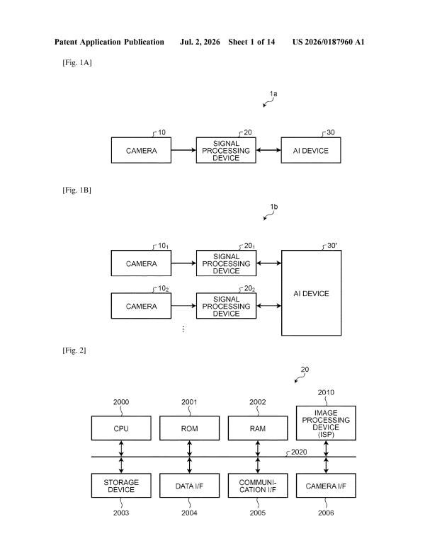
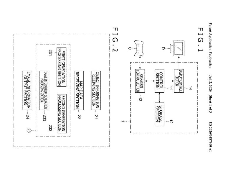
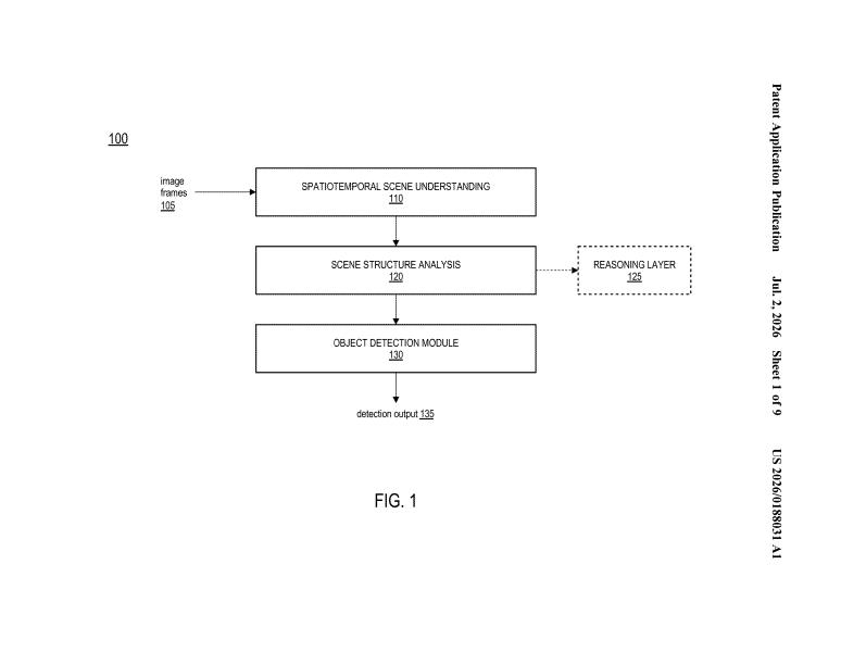
Most computer vision systems recognize objects by matching visual patterns, the same way a child learns to spot a dog from pictures.…

Every Big Tech filing we've broken down, newest first. We read what the major companies publish and cover the ones worth knowing, in plain English.
Most computer vision systems recognize objects by matching visual patterns, the same way a child learns to spot a dog from pictures.…
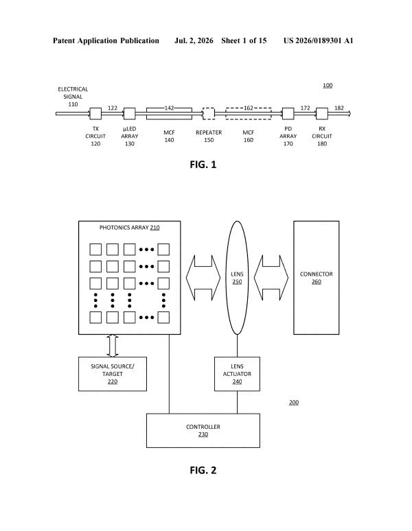
Intel is patenting a way to send data between chips using beams of light instead of electrical signals, and the trick is…
Instead of running AI analysis on an entire image, Sony's latest patent describes a system that zooms in on just the relevant…
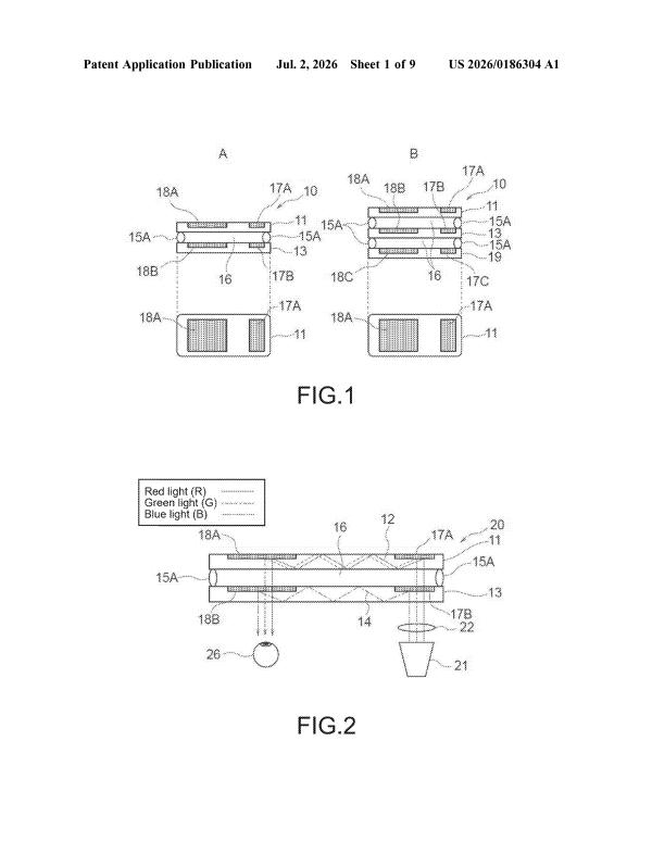
If you've ever tried AR glasses and noticed the world looks slightly tinted or that colors seem off, this Sony patent is…
Keeping a sharp, perfectly framed shot of a sprinter or a flying drone is genuinely hard for conventional cameras. Sony is patenting…
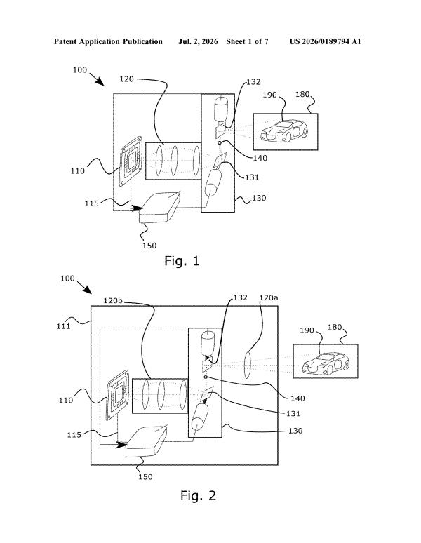
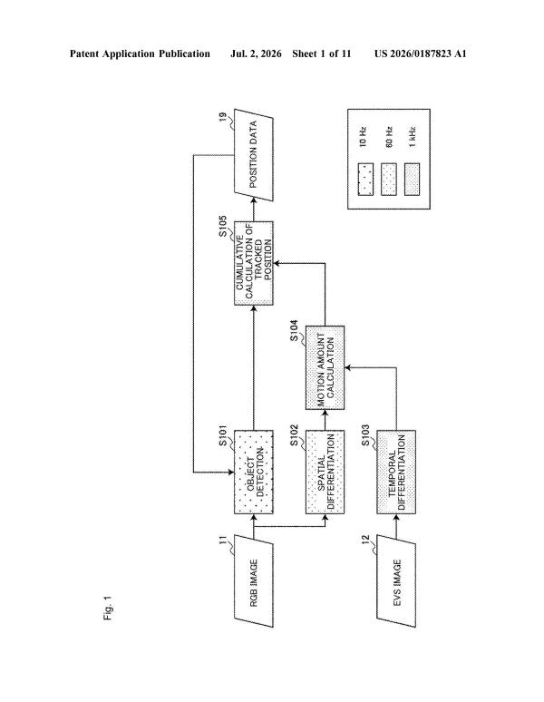
Most cameras have to choose between image detail and speed. Sony's new patent describes a tracking system that uses both at once,…
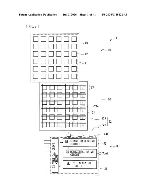
Sony is filing patents on a way to build image sensors from separate stacked layers, each handling a different part of the…
Human skin doesn't just reflect light off its surface, it lets some light in, bounces it around beneath the skin, and sends…
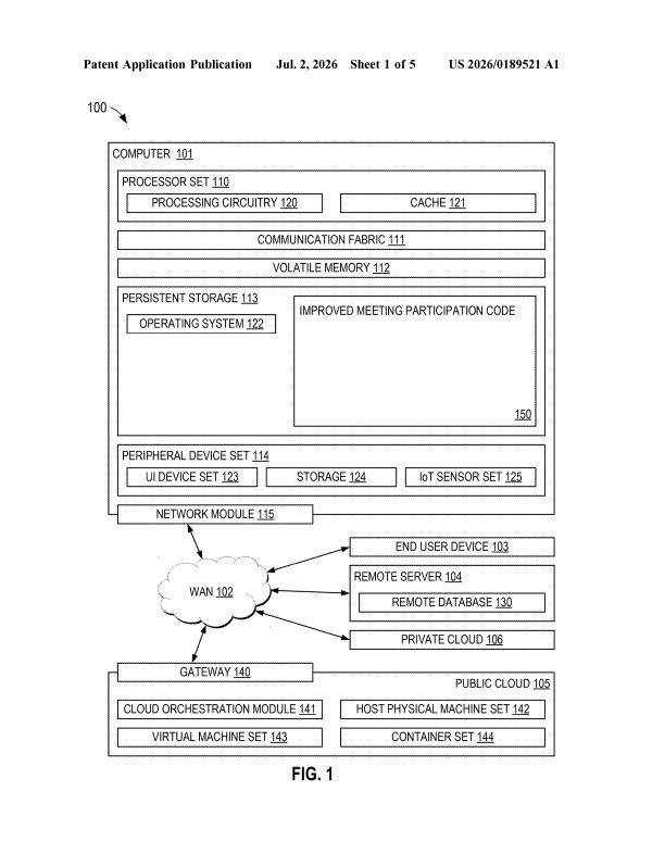
What if missing a meeting meant you could still ask the meeting itself questions afterward? IBM is patenting exactly that: an AI…
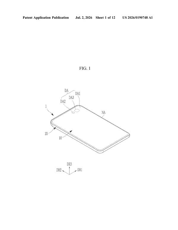
Flexible screens are only as good as the fragile ribbon cables connecting them to the rest of the phone. Samsung Display is…
We read every patent application Big Tech publishes and send you the ones worth knowing. Plain English, free, every week.